

Base plate for stacked packaging
A stacked packaging and substrate technology, applied in semiconductor/solid-state device parts, semiconductor devices, electrical components, etc., can solve the problem of limited interconnection density of upper and lower packaging
- Summary
- Abstract
- Description
- Claims
- Application Information
AI Technical Summary
Problems solved by technology
Method used
Image

Examples
Embodiment Construction
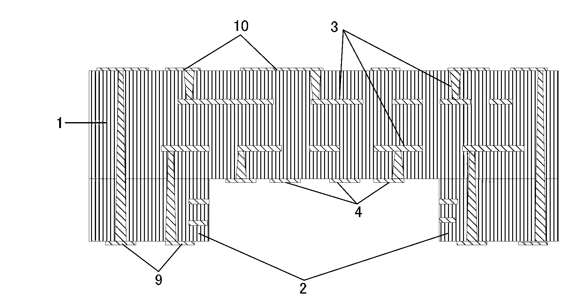
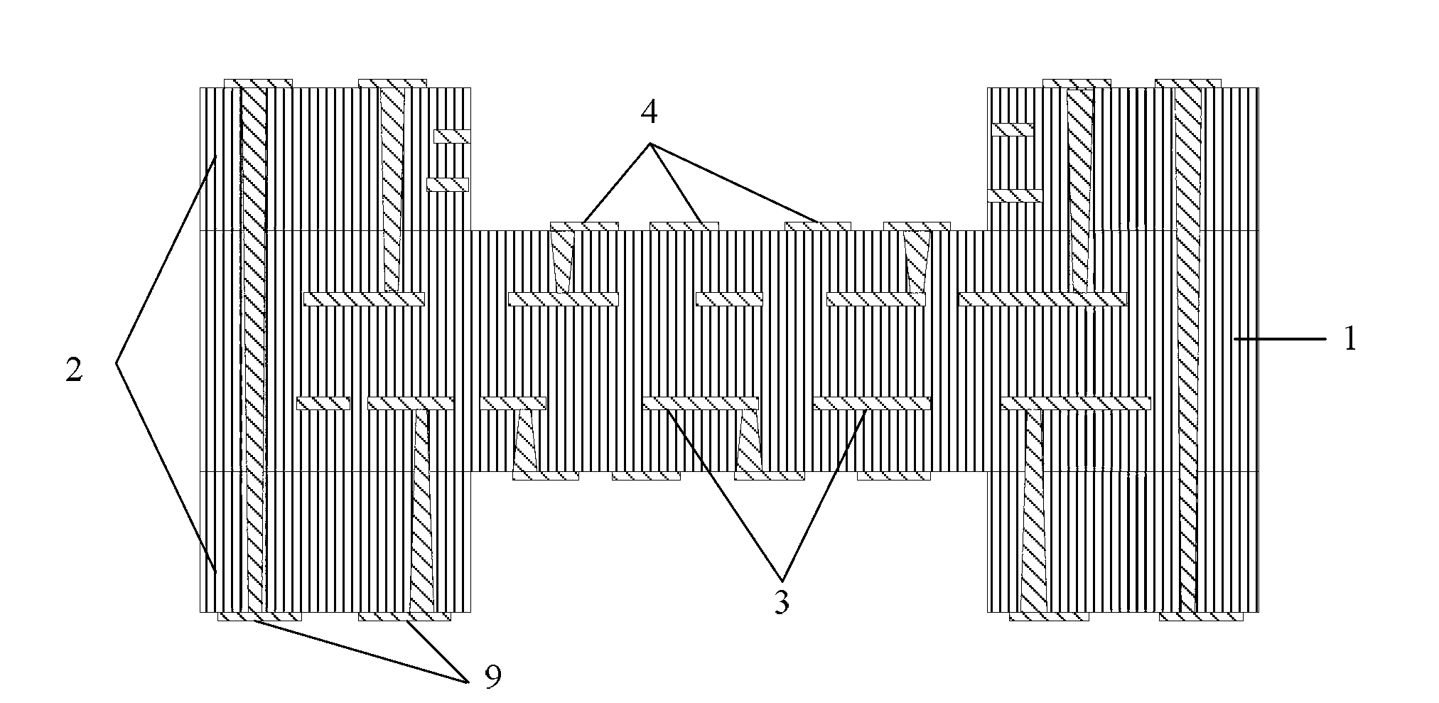
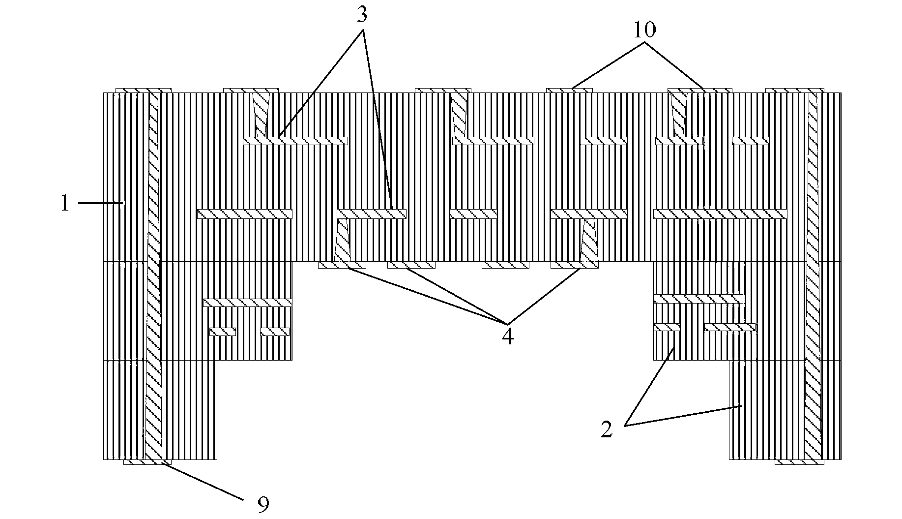
[0023] In the following, in combination with the accompanying drawings in the embodiments of the present invention, the technical solutions in the embodiments of the present invention are clearly and completely expressed mainly by taking the substrate with a first-order cavity on one side as an example. The described embodiments are only part of the implementation of the present invention. example.
[0024] Figures 1 to 3 , are several structural forms of substrates used for stacked packaging provided by the embodiments of the present invention. In order, one side of the substrate has a first-order cavity, both sides have first-order cavities, and one side has second-order cavities. Figure 4 It is a schematic diagram of the structure of the substrate in the case of closed dams in the substrate provided by the embodiment of the present invention.
[0025] The substrate for package-on-package provided by the embodiments of the present invention may be an organic substrate or ...
PUM
 Abstract
Description
Claims
Application Information