Electrostatic protection device

An electrostatic protection and device technology, applied in the field of electrostatic protection devices, can solve problems such as damage to the protection tube and failure of the protection tube to open, and achieve the effects of reducing the turn-on voltage, preventing device failure, and improving electrostatic tolerance.

Inactive Publication Date: 2013-09-18
SHANGHAI HUAHONG GRACE SEMICON MFG CORP
View PDF4 Cites 3 Cited by
  • Summary
  • Abstract
  • Description
  • Claims
  • Application Information

AI Technical Summary

Problems solved by technology

The turn-on voltage is determined by the substrate current and substrate resistance formed by the reverse leakage of the PN junction at the drain end. Because the circuit structure will cause the effective substrate resistance of the NMOS in the middle to be larger than that on both sides, the NMOS in the middle is easier to turn on in advance, and the NMOS in the middle is easier to turn on in advance. At this time, the protective tubes on both sides have not reached the opening condition.
In this way, the turn-on voltage Vt1 of the protective tubes connected in parallel is different. If all the protective tubes cannot be turned on to bleed as much as possible, the protective tubes will be damaged under strong ESD impact.

Method used


Image

  • Electrostatic protection device
  • Electrostatic protection device
  • Electrostatic protection device

Examples


Embodiment Construction

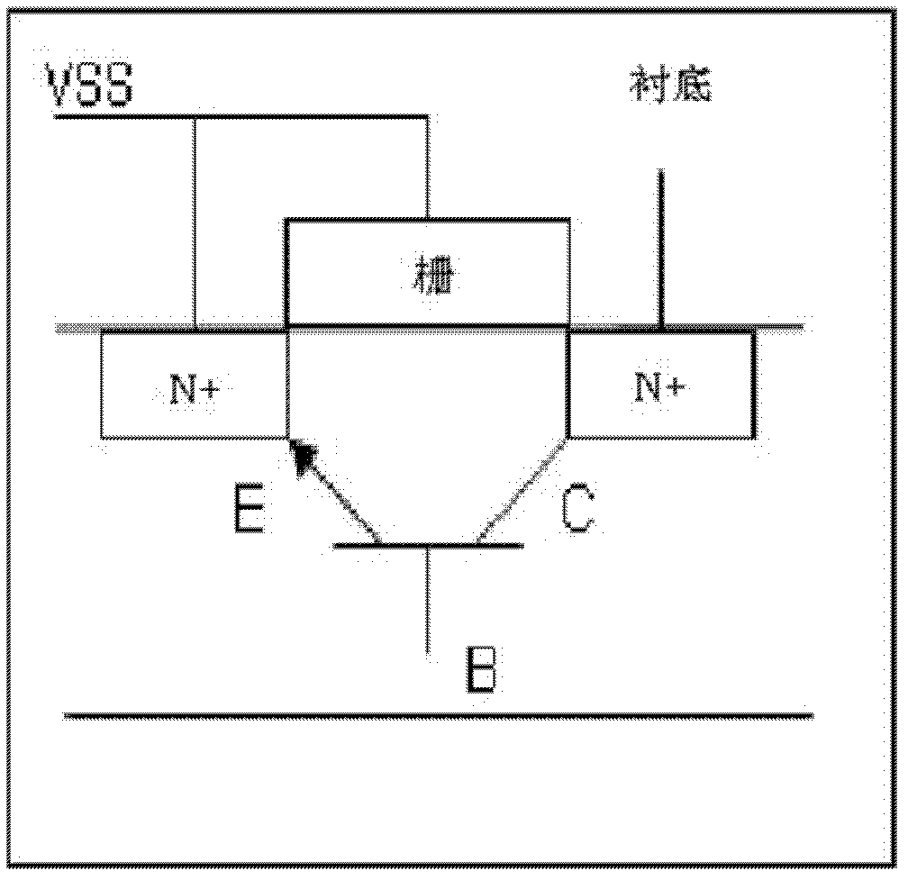
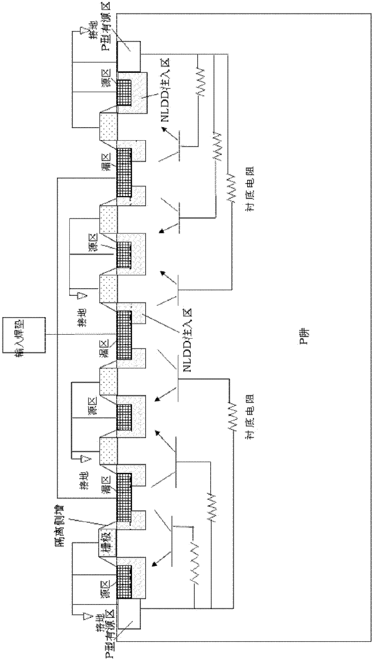
[0020] like image 3 , Figure 4 As shown, the finger-shaped electrostatic protection device of the present invention includes: 2N NMOS structures formed in parallel on the same P well, the outermost side of the paralleled NMOS structures is a source region, and a P-type NMOS structure is formed outside the outermost source region. Active area, common source area / common drain area between adjacent NMOS structures, N≥1; each NMOS structure includes:

[0021] A gate and two isolation spacers are formed on a P well;

[0022] a source region, located in the NLDD injection region on one side of the gate, and the NLDD injection region is located in the P well;

[0023] a drain region, located in the NLDD injection region on the other side of the gate, and the NLDD injection region covers part of the drain region;

[0024] The source / drain region can be formed by N+ implantation;

[0025] All gates, source regions and P-type active regions of this device are grounded, and all dra...


PUM


Abstract

The invention discloses an electrostatic protection device comprising 2N NMOS structures parallelly formed on a P-well, wherein the outmost sides of the parallel NMOS structures are source regions and the outer sides of the outmost-side source regions are formed with P-type active regions; a common source region / a common drain region is formed between adjacent NMOS structures; and N>=1. Each NMOS structure comprises: a gate and two isolation side walls which are all formed on the P-well; a source region which is positioned in an NLDD injection region that is at one side of the gate and the NLDD injection region is in the P-well; a drain region which is positioned in the NLDD injection region at the other side of the gate. The gates, the source regions and the P-type active regions of the protection device are grounded and drain regions are connected to an input-output welding pad terminal; and an NLDD injection block region is formed above each common drain region to block the NLDD injection region formed under the NLDD injection block region. With the electrostatic protection device, the actuation voltage of the electrostatic protection device can be reduced, failure of the device because of a gate-oxide breakdown is prevented and static endurance of the electrostatic protection device is improved.

Description

technical field [0001] The invention relates to the field of integrated circuit manufacturing, in particular to an electrostatic protection device. Background technique [0002] Static electricity is an objective natural phenomenon, which can be produced in many ways, such as contact, friction, induction between electrical appliances, etc. Static electricity is characterized by long-term accumulation, high voltage, low power, small current and short action time. Static electricity causes serious harm in many fields. Friction electrification and human body static electricity are two major hazards in the electronics industry, which often cause unstable operation or even damage of electronic and electrical products. ESD is a discipline formed since the middle of the 20th century to study the generation, harm and protection of static electricity. It is customary in the world to refer to the equipment used for electrostatic protection as ESD. [0003] Today's popular process t...

Claims


Application Information

Patent Timeline
Patent Type & Authority Applications(China)
IPC IPC(8): H01L27/02
Inventor 苏庆徐向明王邦磷邓樟鹏
Owner SHANGHAI HUAHONG GRACE SEMICON MFG CORP
Why Eureka
Try Eureka