Organic light-emitting diode display panel and production method thereof
A technology for light-emitting diodes and display panels, which is applied in the fields of organic semiconductor devices, semiconductor/solid-state device manufacturing, electrical components, etc., and can solve the problems of uneven brightness, unavailability, and uniform driving voltage.
- Summary
- Abstract
- Description
- Claims
- Application Information
AI Technical Summary
Problems solved by technology
Method used
Image

Examples
no. 1 example
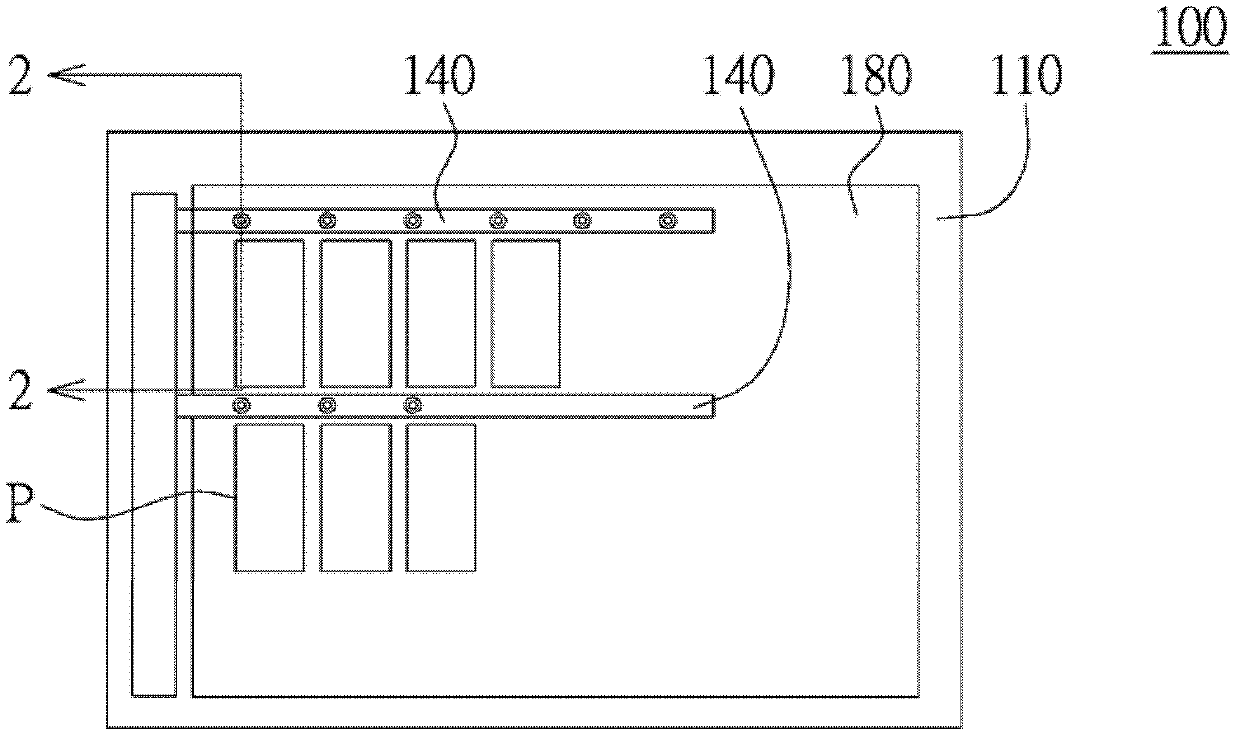
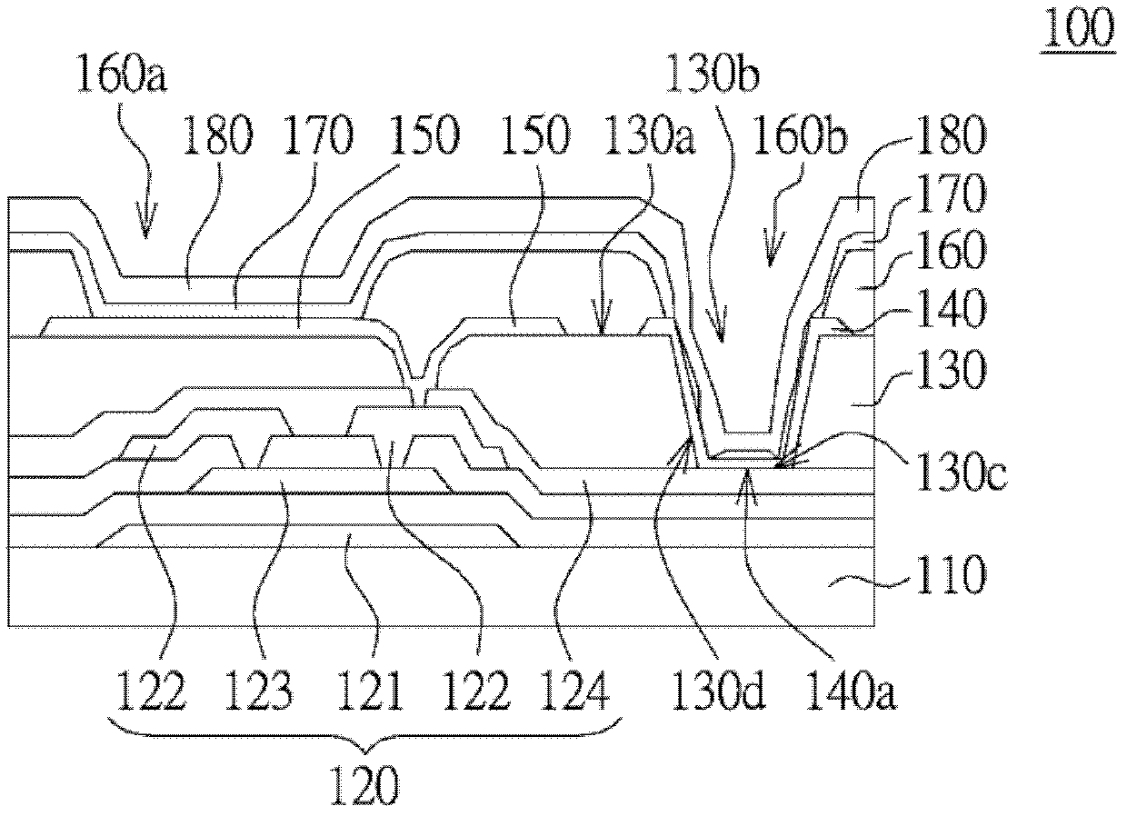
[0046] Please refer to Figure 1~2 , figure 1 A top view of the organic light emitting diode display panel 100 of the first embodiment is shown, figure 2 draw figure 1 A cross-sectional view of the OLED display panel 100 along the section line 2-2. The OLED display panel 100 includes a substrate 110 , a thin film transistor 120 , a flat layer 130 , an auxiliary electrode layer 140 , a reflective electrode layer 150 , a pixel definition layer 160 , an organic light emitting layer 170 and a transparent electrode layer 180 . In this embodiment, the OLED display panel 100 is a top emission type. Such as figure 2 As shown, the material of the substrate 110 is, for example, glass or silicon (Si). The stack structure of the organic light emitting diode display panel 100 is sequentially formed on the substrate 110 through various procedures of the semiconductor process.
[0047] Such as figure 2 As shown, the thin film transistor 120 is disposed on the substrate 110 to provi...
no. 2 example
[0062] Please refer to Figure 8-9 , Figure 8 A top view of the organic light emitting diode display panel 200 of the second embodiment is shown, Figure 9 draw Figure 8 A schematic diagram of the OLED display panel 200 along the section line 9-9. The difference between the OLED display panel 200 of this embodiment and the OLED display panel 100 of the first embodiment lies in the design of the groove 230b, and the rest of the similarities will not be described again.
[0063] Such as Figure 9 As shown, the planar layer 230 has several cavities 230e. The plurality of concave holes 230e are disposed in the groove 230b. That is to say, the bottom 230c of the groove 230b is not flat but uneven. Since the bottom 230c of the groove 230b is uneven, the organic light-emitting layer 270 is discontinuously laid on the auxiliary electrode layer 240, so the transparent electrode layer 280 can still contact the auxiliary electrode layer 240, thereby reducing the impedance between...
no. 3 example
[0068] Please refer to Figure 12 , which shows Figure 13 A cross-sectional view of the OLED display panel 300 . The difference between the OLED display panel 300 of this embodiment and the OLED display panel 200 of the second embodiment lies in the design of the groove 330b, and the rest of the similarities will not be described again.
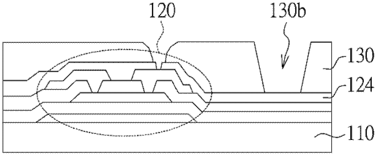
[0069] Such as Figure 12 As shown, the groove 330 b runs through the planar layer 330 and a portion of the dielectric layer 324 . And the metal layer 322 used to make the thin film transistor 320 remains at the bottom 330c of the groove 330b, and several cavities 330e are formed in the groove 330b. Steeper slopes can be created with this design. Since the bottom 330c of the groove 330b is uneven, the organic light-emitting layer 370 is discontinuously laid on the auxiliary electrode layer 340, so the transparent electrode layer 380 can still contact the auxiliary electrode layer 340, thereby reducing the impedance between the two. .
...
PUM
| Property | Measurement | Unit |
|---|---|---|
| Diameter | aaaaa | aaaaa |
Abstract
Description
Claims
Application Information
 - Generate Ideas
- Intellectual Property
- Life Sciences
- Materials
- Tech Scout
- Unparalleled Data Quality
- Higher Quality Content
- 60% Fewer Hallucinations
Browse by: Latest US Patents, China's latest patents, Technical Efficacy Thesaurus, Application Domain, Technology Topic, Popular Technical Reports.
© 2025 PatSnap. All rights reserved.Legal|Privacy policy|Modern Slavery Act Transparency Statement|Sitemap|About US| Contact US: help@patsnap.com