Unlock instant, AI-driven research and patent intelligence for your innovation.

Spacer and manufacturing method thereof, substrate and display device

A manufacturing method and technology for spacers, which are applied in the directions of exposure devices, optics, instruments, etc. in photolithography processes, can solve problems such as increasing production costs, large spacers, and increasing backlight costs, thereby reducing production costs and complexity. The effect of increasing the aperture ratio

Active Publication Date: 2013-10-02
HEFEI BOE OPTOELECTRONICS TECH +1
View PDF4 Cites 5 Cited by
  • Summary
  • Abstract
  • Description
  • Claims
  • Application Information

AI Technical Summary

Problems solved by technology

[0005] The existing manufacturing method of the spacer needs to use a half-tone mask or a gray-tone mask for exposure, which increases the complexity of the process and increases the production cost; and is affected by the exposure accuracy, the size of the spacer is Relatively large, resulting in a smaller aperture ratio of the display panel, increasing the cost of the backlight

Method used


Image

  • Spacer and manufacturing method thereof, substrate and display device
  • Spacer and manufacturing method thereof, substrate and display device

Examples


Embodiment 1

[0051] In this embodiment, spacers of various heights can be formed on the substrate, where the substrate can be an array substrate or a color filter substrate. This embodiment specifically includes the following steps:

[0052] Step a1: forming a photosensitive material solution, the main components of the photosensitive material solution are the first transparent polymer or its monomer, and a photoinitiator, wherein the first transparent polymer and its monomer do not infiltrate the substrate, and the first transparent polymer The molecular weight range can be several thousand to millions, specifically, the first transparent polymer can be selected from styrene resin;

[0053] Step a2: Spin-coat or scrape-coat the photosensitive material solution on the substrate to form a layer of photosensitive material film, wherein the size of the spacer can be reduced by controlling the thickness of the photosensitive material film. The smaller the thickness of the photosensitive materi...

Embodiment 2

[0059] In this embodiment, spacers of various heights can be formed on the substrate, where the substrate can be an array substrate or a color filter substrate. This embodiment specifically includes the following steps:

[0060] Step b1: forming a photosensitive material solution, adding the first transparent polymer or its monomers to the existing acrylic resin mixture solution used to prepare spacers to form a photosensitive material solution, wherein the first transparent polymer and the acrylic resin are mutually incompatible Infiltration, the molecular weight range of the first transparent polymer can be several thousand to millions, specifically, the first transparent polymer can be selected from styrene resin;

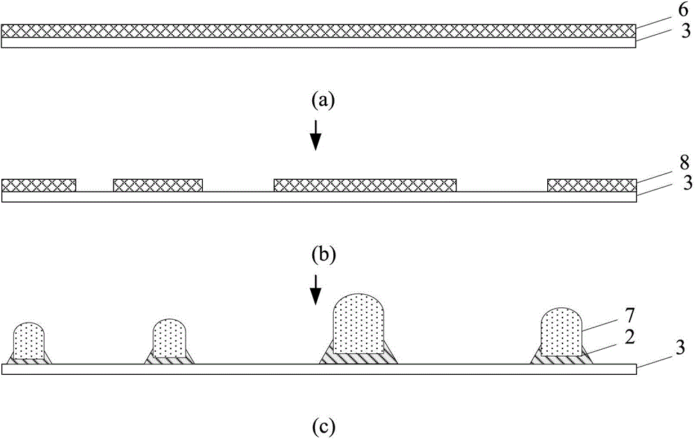
[0061] Step b2: if figure 2 As shown in (a), the photosensitive material solution is spin-coated or scraped-coated on the substrate 3 to form a layer of photosensitive material film 6, wherein the size of the spacer can be reduced by controlling the thickness ...


PUM


Abstract

The invention provides a spacer and a manufacturing method thereof, a substrate and a display device and belongs to the technical field of display. The manufacturing method of the spacer comprises the following steps of forming a photosensitive material thin film used for manufacturing the spacer on the substrate, wherein a photosensitive material contains a first transparent polymer or a monomer thereof, the first transparent polymer does not infiltrate the substrate; exposing and developing the photosensitive material thin film, and forming a plurality of spacer graphs with different dimensions on the substrate; and heating the substrate on which the spacer graphs are formed under preset temperature, and then, cooling to enable the spacer graphs to protrude to form the spacers, wherein the spacer graphs with different dimensions form the spacers with different heights. According to the technical scheme provided by the invention, the aperture opening ratio of the display device can be increased, and the production cost can be reduced.

Description

technical field [0001] The invention relates to the field of display technology, in particular to a spacer, a manufacturing method thereof, a substrate and a display device. Background technique [0002] The display panel of a TFT LCD (Thin Film Transistor Liquid Crystal Display) is usually composed of an array substrate, a liquid crystal layer and a color filter substrate. In order to control the thickness and uniformity of the liquid crystal layer, the color filter substrate or array substrate A spacer (Post Spacer, PS) is formed on it to ensure the thickness of the liquid crystal cell. [0003] In the prior art, acrylic resin mixture solutions are often used to prepare spacers. The main components of acrylic resin mixture solutions are acrylic resins or acrylic resin monomers and photoinitiators. The acrylic resin mixture solutions are photosensitive materials. The quasi-mixture solution is coated on the substrate, and spacers can be formed through processes such as expo...

Claims


Application Information

Patent Timeline
IPC IPC(8): G02F1/1339G03F7/20
CPCG02F1/13394G02F1/13398
Inventor 李红敏李小和刘永张晓洁
Owner HEFEI BOE OPTOELECTRONICS TECH
Features
  • R&D
  • Intellectual Property
  • Life Sciences
  • Materials
  • Tech Scout
  • Unparalleled Data Quality
  • Higher Quality Content
  • 60% Fewer Hallucinations
Learn More