Input signal protection circuit based on power carrier communication
A technology of power carrier communication and input signal, applied in distribution line transmission system and other directions, can solve the problems of large harmonic component of input signal, lower communication success rate, lower transmission efficiency, etc., so as to improve the signal-to-noise ratio and ensure successful communication. efficiency, improve efficiency
- Summary
- Abstract
- Description
- Claims
- Application Information
AI Technical Summary
Problems solved by technology
Method used
Image
Examples
Embodiment 1
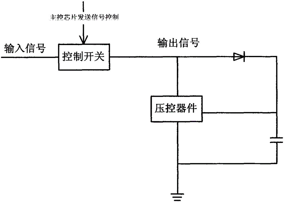
[0018] Such as Figure 4 As shown, the input signal protection circuit based on power carrier communication according to the present invention includes: a control switch NFET2, a voltage control device NFET1, a diode VT2 and a capacitor C1. When in the sending state, the external main control chip sends a control signal to turn off NFET2, preventing the circuit on the receiving side from becoming a load on the sending side, thereby improving the sending efficiency of the output terminal. When in the receiving state, the control signal turns on NFET2. After rectification and filtering by VT2 and C1, the amplitude signal of the input signal is detected. This signal can directly control the internal resistance of NFET1, thereby pulling down the amplitude of the output signal. Finally, a function of amplitude control is realized.
PUM
 Abstract
Description
Claims
Application Information


