LCD panel, drive method and LCD device

A technology of liquid crystal panel and driving method, applied in static indicators, nonlinear optics, instruments, etc.

Active Publication Date: 2013-10-09
TCL CHINA STAR OPTOELECTRONICS TECH CO LTD
View PDF8 Cites 21 Cited by
  • Summary
  • Abstract
  • Description
  • Claims
  • Application Information

AI Technical Summary

Problems solved by technology

And because the data lines and the pixel capacitors connected to them have relatively large capacitance, the power consumption of the data drive circuit accounts for the vast majority of the entire drive circuit. How to reduce the dynamic power consumption of the data drive circuit has become a research hotspot.

Method used


Image

  • LCD panel, drive method and LCD device
  • LCD panel, drive method and LCD device
  • LCD panel, drive method and LCD device

Examples


Embodiment 1

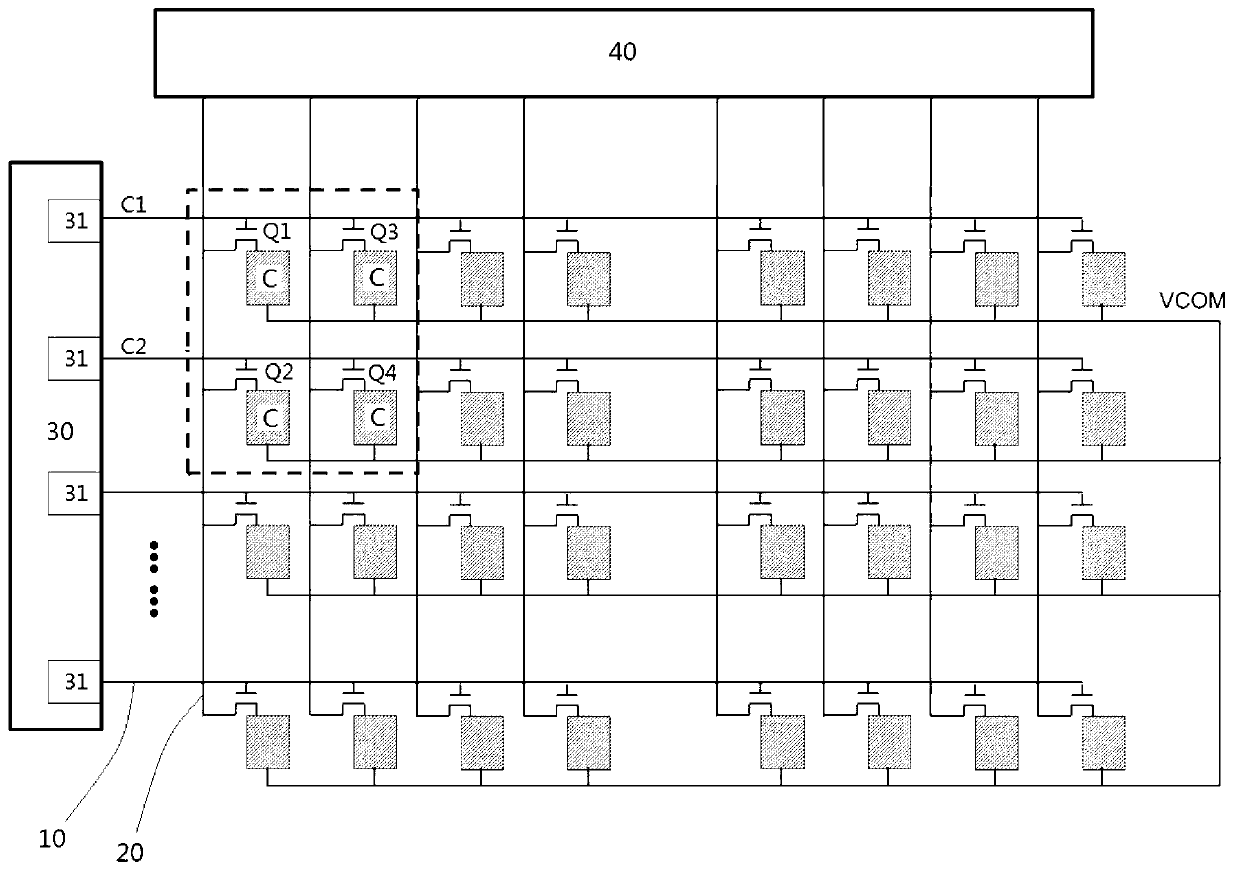
[0040] Such as figure 2 As shown, the liquid crystal panel includes a plurality of thin film transistors, crisscrossed scan lines 10 and data lines 20, a scan driving chip 30 driving the scan lines 10, and a data driving chip 40 driving the data lines 20; the gate of each row of TFTs is connected to one In the scan line 10, the source of each TFT is connected to a data line 20, and the drain of each TFT is connected to a pixel electrode. The scan driving chip 30 includes a compensation driving unit 31 coupled to the scan line 10.

[0041] The compensation driving unit 31 drives the thin film transistor corresponding to the scan line C2 of the next row to be turned on when or after the scan driving chip 30 drives the thin film transistor corresponding to the current scan line C1 to conduct, and the thin film transistor corresponding to the current scan line C1 receives The thin film transistor corresponding to the next row of scan line C2 is turned off when the data signal of the ...

Embodiment 2

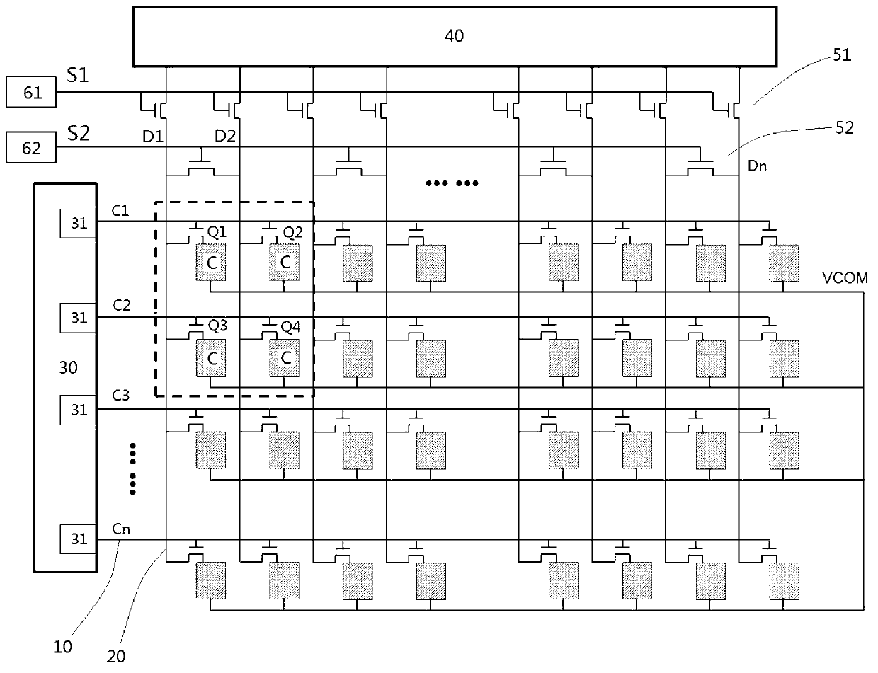
[0047] Such as image 3 As shown, this embodiment discloses a method for driving a liquid crystal panel. The liquid crystal panel includes a plurality of thin film transistors, crisscrossed scan lines and data lines, a scan driving chip for driving the scan lines, and a data driving chip for driving the data lines; The gate of each row of TFTs is connected to a scan line, the source of each column of TFTs is connected to a data line, and the drain of each TFT is connected to a pixel electrode; the driving method includes:

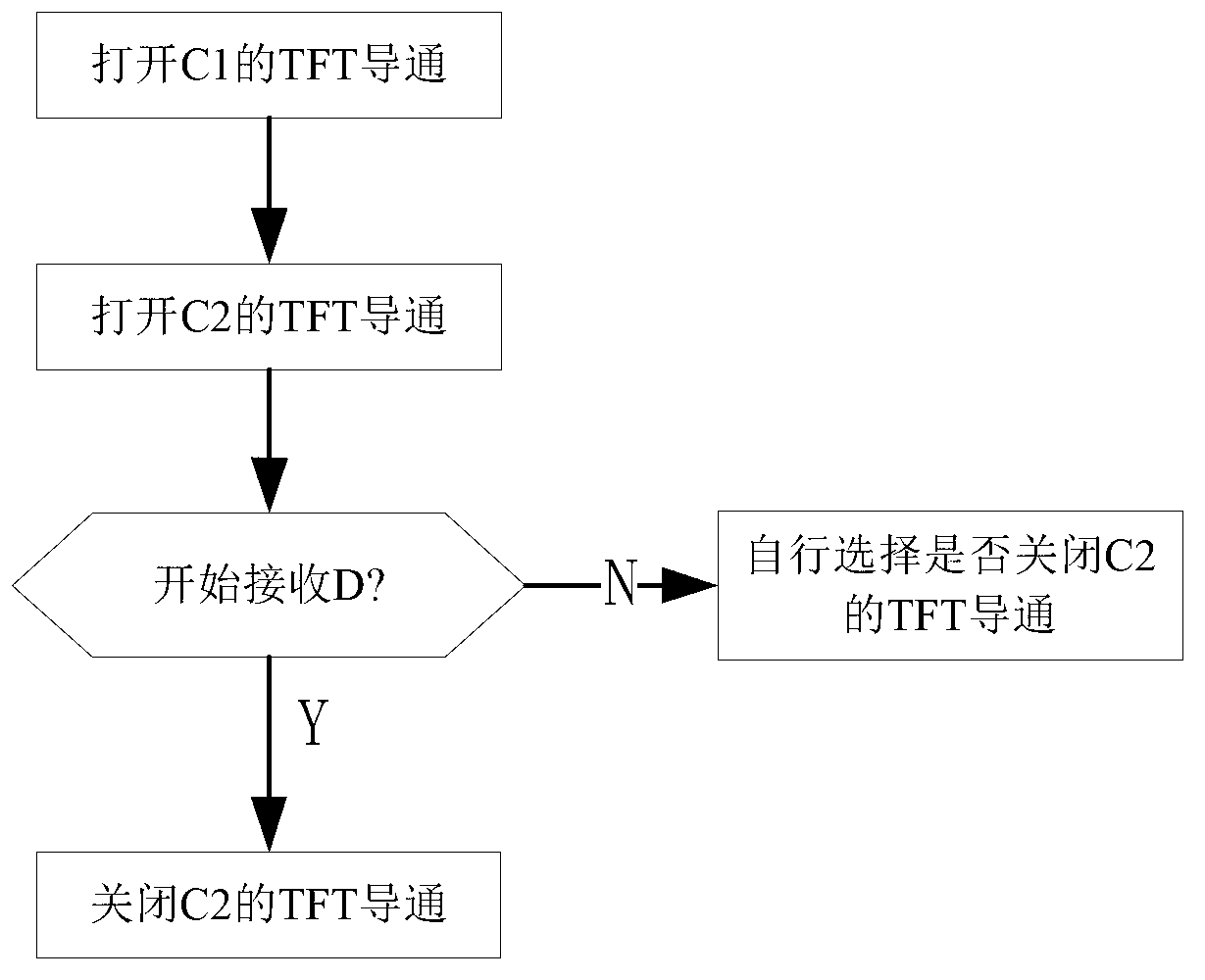
[0048] A. The scan driving chip drives the thin film transistor corresponding to the current scan line C1 to turn on;

[0049] B. The scan driving chip drives the thin film transistor corresponding to the next row of scan line C2 to turn on;

[0050] C. Determine whether the thin film transistor corresponding to the current scan line starts to receive the data driving signal of the data drive chip D, and drive the next row of scan line when or before the thin film...


PUM


Abstract

The invention discloses an LCD panel, a drive method and an LCD device. The LCD panel comprises a plurality of thin film transistors, scanning lines and data lines which are arranged in a criss-cross mode, a scanning drive chip driving the scanning lines and a data drive chip driving the data lines. Gate electrodes of each row of the thin film transistors are connected with one scanning line, and source electrodes of each line of the thin film transistors are connected with one data line. A drain electrode of each thin film transistor is connected with a pixel electrode. The scanning drive chip comprises a compensation drive unit which is coupled with the scanning lines. When or after the compensation drive unit drives the scanning drive chip to drive the corresponding thin film transistors of the current scanning line to be conducted, the corresponding thin film transistors of the next scanning line are driven to be conducted. When or before the corresponding thin film transistors of the current scanning line receive data signals of the data drive chip, the corresponding thin film transistors of the next scanning line are closed. The LCD panel, the drive method and the LCD device can reduce power consumption of a data drive circuit.

Description

Technical field [0001] The present invention relates to the field of liquid crystal display, and more specifically, to a liquid crystal panel, a driving method and a liquid crystal display device. Background technique [0002] The liquid crystal display device includes a liquid crystal panel and a backlight module that provides a light source for the liquid crystal panel. The liquid crystal panel includes a plurality of thin film transistors (TFT), and criss-crossed scan lines and data lines. The scan lines of each row control the gate of a row of TFTs. The data lines of each column are connected to the source of a column of TFTs. The drain is connected to a pixel electrode to form a pixel capacitor. The pixel capacitor includes a pixel electrode and a common electrode opposite to each other. The pixel electrode is connected to the drain of the TFT, and the common electrode is generally connected to a constant voltage signal. The pixel electrode and the common electrode are fill...

Claims


Application Information

Patent Timeline
Patent Type & Authority Applications(China)
IPC IPC(8): G02F1/1362G02F1/1368G02F1/133G09G3/36
CPCG09G3/3688G09G2310/0251
Inventor 朱江
Owner TCL CHINA STAR OPTOELECTRONICS TECH CO LTD
Why Eureka
Try Eureka