Method for erasing split gate type flash memory
A split-gate flash memory and control gate technology, applied in the field of memory, can solve the problems of fast degradation speed of tunnel oxide layer and low flash memory durability, and achieve the effects of reducing voltage stress, slowing down degradation speed, and improving durability
- Summary
- Abstract
- Description
- Claims
- Application Information
AI Technical Summary
Problems solved by technology
Method used
Image
Examples
Embodiment Construction
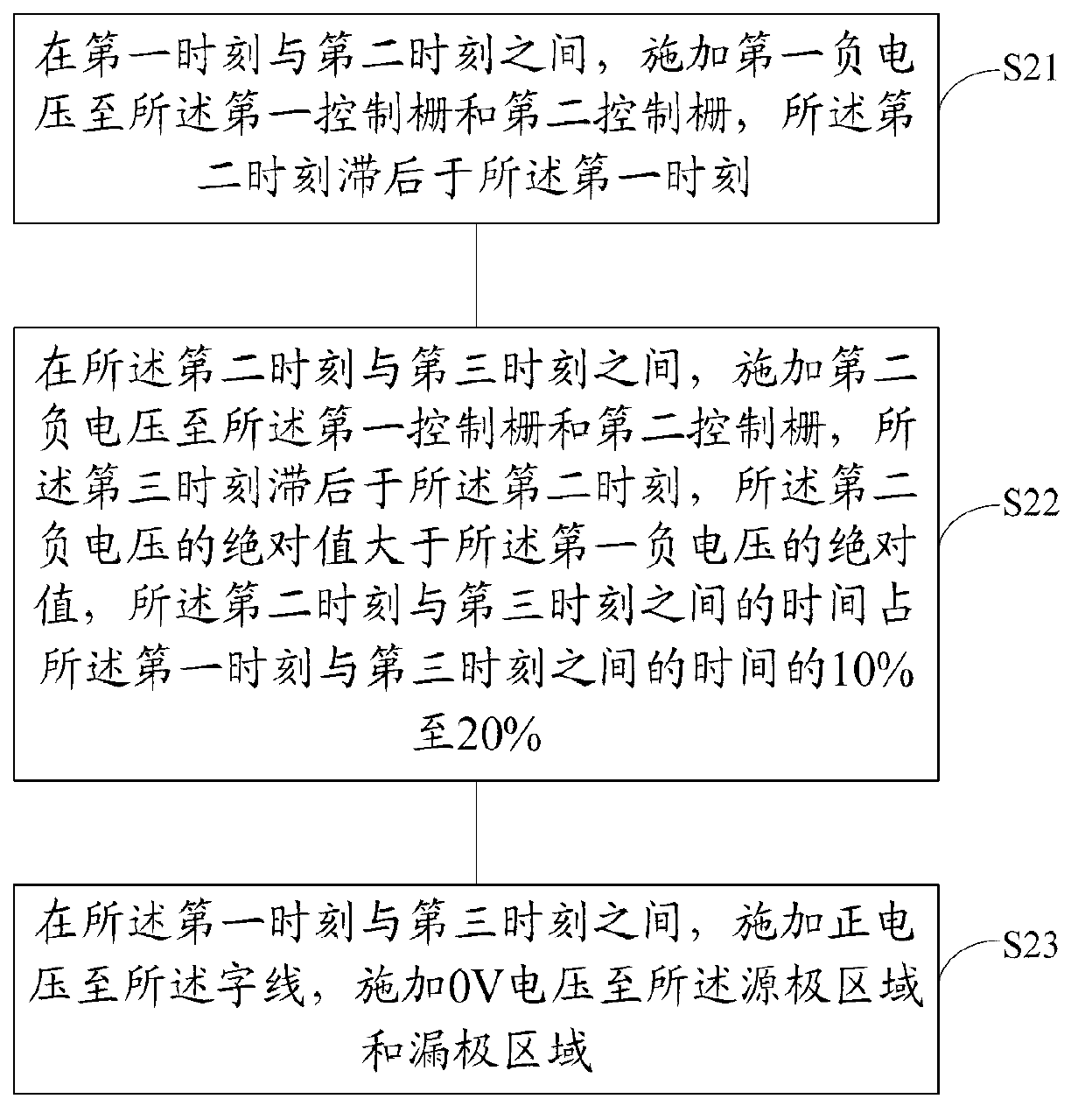
[0022] As described in the background art, when the split-gate flash memory is erased, the tunnel oxide layer in the split-gate flash memory bears a large voltage stress, which causes degradation of the tunnel oxide layer, and thus Reduce the durability of the entire flash memory. After research, the inventor of the technical solution provided a method for erasing split-gate flash memory.
[0023] In order to make the above-mentioned objects, features and advantages of the present invention more obvious and understandable, the specific embodiments of the present invention will be described in detail below with reference to the accompanying drawings.
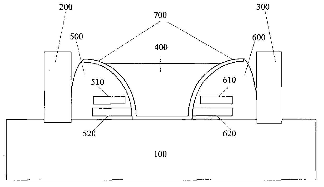
[0024] figure 1 It is a schematic diagram of the cross-sectional structure of the split-gate flash memory according to the present invention. reference figure 1 , The split-gate flash memory includes: a semiconductor substrate 100 having a source region 200 and a drain region 300 spaced apart on the semiconductor substrate 100; a wor...
PUM
 Abstract
Description
Claims
Application Information
 - R&D
- Intellectual Property
- Life Sciences
- Materials
- Tech Scout
- Unparalleled Data Quality
- Higher Quality Content
- 60% Fewer Hallucinations
Browse by: Latest US Patents, China's latest patents, Technical Efficacy Thesaurus, Application Domain, Technology Topic, Popular Technical Reports.
© 2025 PatSnap. All rights reserved.Legal|Privacy policy|Modern Slavery Act Transparency Statement|Sitemap|About US| Contact US: help@patsnap.com


