
A silicon based mems microphone, a system and a package with the same

A microphone, silicon-based technology, applied in the field of microphones, can solve problems such as easy trapping in microphones, diaphragm damage, etc.

Active Publication Date: 2013-10-09
WEIFANG GOERTEK MICROELECTRONICS CO LTD
View PDF5 Cites 45 Cited by
  • Summary
  • Abstract
  • Description
  • Claims
  • Application Information

AI Technical Summary

Problems solved by technology

[0007] However, as can be seen from the above description, whether it is a separate conventional MEMS microphone or a conventional MEMS microphone package, there are problems
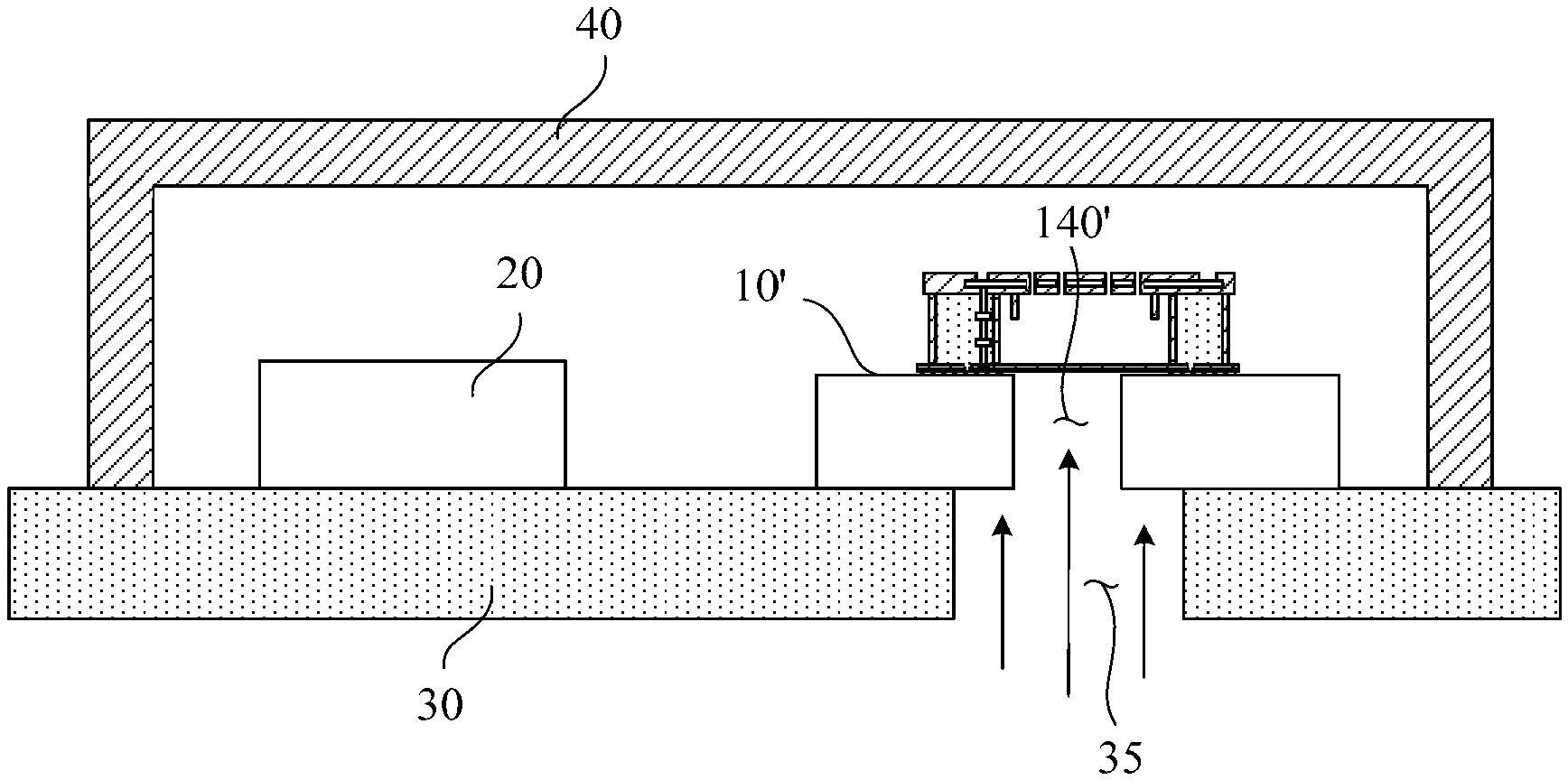
For structures with an open back hole in the base of a conventional microphone and / or an acoustic hole on the PCB, the diaphragm of a conventional microphone is susceptible to damage due to air pressure pulses e.g. Foreign matter such as particles are easily trapped inside the microphone through the back hole and / or the sound hole

Method used


Image

  • A silicon based mems microphone, a system and a package with the same
  • A silicon based mems microphone, a system and a package with the same
  • A silicon based mems microphone, a system and a package with the same

Examples


no. 1 example )

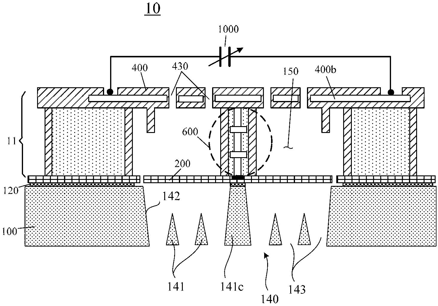
[0032] figure 2 is a sectional view showing the structure of the silicon-based MEMS microphone according to the first embodiment of the present invention. MEMS microphones can receive acoustic signals and convert the received acoustic signals into electrical signals for subsequent processing and output. like figure 2As shown, the silicon-based MEMS microphone 10 described in the first embodiment of the present invention may include a silicon substrate 100 and an acoustic sensing part 11 supported on the silicon substrate 100, wherein, between the silicon substrate 100 and the acoustic sensing part 11 An insulating oxide layer 120 is interposed therebetween. The acoustic sensing part 11 in the microphone 10 may at least include: a conductive and compliant diaphragm 200 , a perforated back plate 400 and an air gap 150 . Diaphragm 200 is formed using a portion of a silicon device layer such as a top silicon film on a silicon-on-insulator (SOI) wafer or using a polysilicon (P...

no. 2 example )

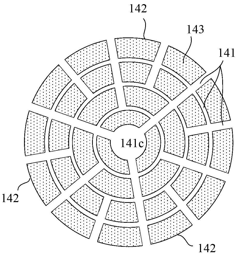
[0039] Image 6 is a cross-sectional view showing the structure of the silicon-based MEMS microphone according to the second embodiment of the present invention, Figure 7 is the floor plan, showing the Image 6 An exemplary pattern of network structure backholes formed in the silicon substrate when viewed from the bottom of the silicon substrate of the microphone in .

[0040] Will Image 6 and figure 2 In contrast, the difference between the acoustic sensing part of the microphone according to the second embodiment of the present invention and the acoustic sensing part of the microphone according to the first embodiment is that, in the second embodiment, the acoustic sensing part of the microphone 10 The sensing part 11 may also include an interconnection column 600, which is arranged between the edge of the diaphragm 200 and the edge of the back plate 400 to electrically lead the diaphragm outward by using a CMOS metal interconnection method, and the diaphragm 200 The ...


PUM


Abstract

A silicon based MEMS microphone comprises a silicon substrate (100) and an acoustic sensing part (11) supported on the silicon substrate, wherein a mesh-structured back hole (140) is formed in the substrate and aligned with the acoustic sensing part, the mesh-structured back hole includes a plurality of mesh beams (141) which are interconnected with each other and supported on the sidewall (142) of the mesh-structure back hole, the plurality of mesh beams and the side wall define a plurality of mesh holes (143) which all have a tapered profile and merge into one hole in the vicinity of the acoustic sensing part at the top side of the silicon substrate. The mesh-structured back hole can help to streamline the air pressure pulse caused, for example, in a drop test and thus reduce the impact on the acoustic sensing part of the microphone, and also serve as a protection filter to prevent alien substances such as particles entering the microphone.

Description

technical field [0001] The invention relates to the technical field of microphones, in particular to a silicon-based MEMS microphone. Background technique [0002] Silicon-based MEMS microphones, also known as acoustic transducers, have been in development for many years. Silicon-based MEMS microphones can be widely used in many applications, such as mobile phones, tablets, cameras, hearing aids, smart toys, due to their potential advantages in miniaturization, performance, reliability, environmental durability, cost, and mass production capability and monitoring devices. [0003] In general, silicon-based MEMS microphones include a fixed perforated backplate and a highly compliant diaphragm with an air gap formed between the backplate and the diaphragm. The perforated backplate and the compliant diaphragm constituting the variable air gap capacitor are usually formed on a single silicon substrate, one of which is directly exposed to the outside through a back hole formed ...

Claims


Application Information

Patent Timeline
IPC IPC(8): B81B7/00B81C1/00H04R19/04H04R7/00
CPCB81B7/00H04R7/04H04R2201/003B81C1/00B81B7/0061H04R1/02H04R19/04H04R2201/02H04R19/005B81B2201/0257H04R2207/00H04R1/086H01L2924/1461
Inventor 王喆蔡孟锦
Owner WEIFANG GOERTEK MICROELECTRONICS CO LTD
Learn More