Method for forming semiconductor device and method for forming fin field effect transistor
A technology of semiconductors and devices, which is applied in the field of semiconductor manufacturing, can solve problems such as device performance problems, and achieve the effect of stable performance and high precision
- Summary
- Abstract
- Description
- Claims
- Application Information
AI Technical Summary
Problems solved by technology
Method used
Image

Examples
Embodiment Construction
[0048] As mentioned in the background, there are problems with the device performance of the FinFET in the prior art.
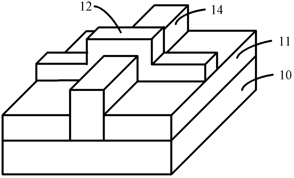
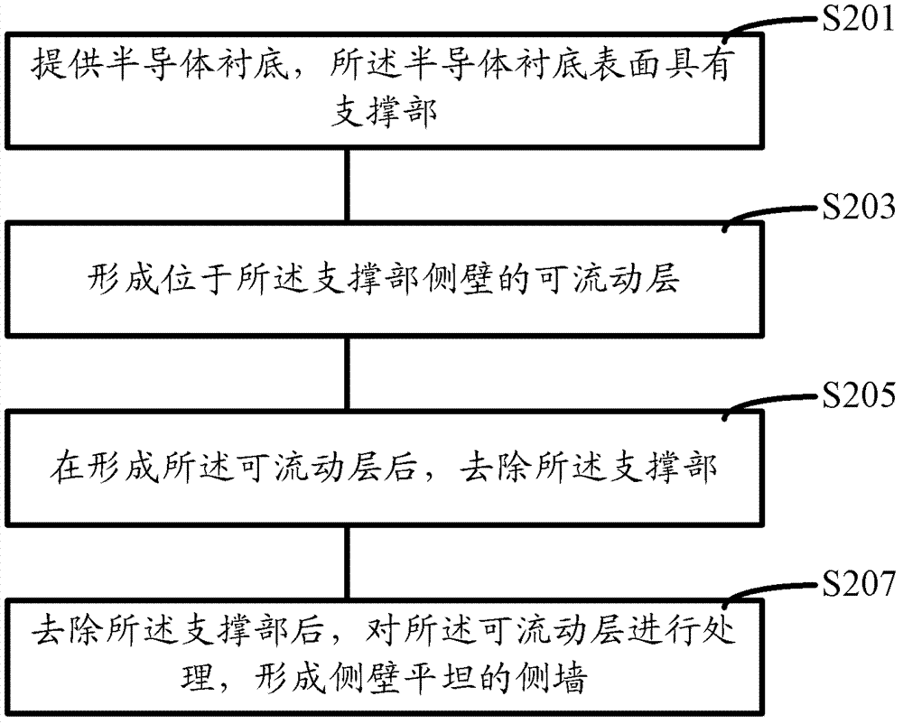
[0049] After research, the inventors have found that one of the reasons for the device performance problems of the prior art fin field effect transistors is that the supporting part is formed by using an etching process, the sidewall is formed on the side wall of the supporting part, and then the side wall is formed by the sidewall When the wall is used as a mask to etch the hard mask layer and the semiconductor substrate to form the fin, the side wall of the support part is corroded by the etching gas, and the side wall of the formed support part is uneven, and the side wall is uneven. When the support part is used as a support to form a side wall, the side wall of the formed side wall close to the support part also has unevenness, and when the support part is subsequently removed, the side wall of the side wall close to the support part is still uneven, even...
PUM
 Abstract
Description
Claims
Application Information
PatSnap Eureka turns technology decisions into work you can execute. Powered by our Innovation Knowledge Graph, it runs expert workflows across engineering, life sciences, materials and intellectual property. Get your review-ready output in minutes.


