
Capacitive MEMS acceleration sensor

An acceleration sensor and acceleration sensing technology, which is applied in the directions of measurement of acceleration, multi-dimensional acceleration measurement, speed/acceleration/shock measurement, etc., can solve problems such as cracked shell, broken lead wire, poor packaging reliability, etc., and reduce the cost of cutting and bonding Difficulty, improved sensitivity of induction, and beneficial effect of chip arrangement

Active Publication Date: 2015-05-20
MIRAMEMS SENSING TECH CO LTD
View PDF3 Cites 0 Cited by
  • Summary
  • Abstract
  • Description
  • Claims
  • Application Information

AI Technical Summary

Problems solved by technology

Practice has shown that the existing sensor packaging technology generally has the problems of poor resistance to high overload, low natural frequency, and poor packaging reliability. , there are often problems such as shell cracking, cover plate depression, chip falling off from the shell substrate, lead wire breakage, etc.

Method used


Image

  • Capacitive MEMS acceleration sensor
  • Capacitive MEMS acceleration sensor
  • Capacitive MEMS acceleration sensor

Examples


Embodiment

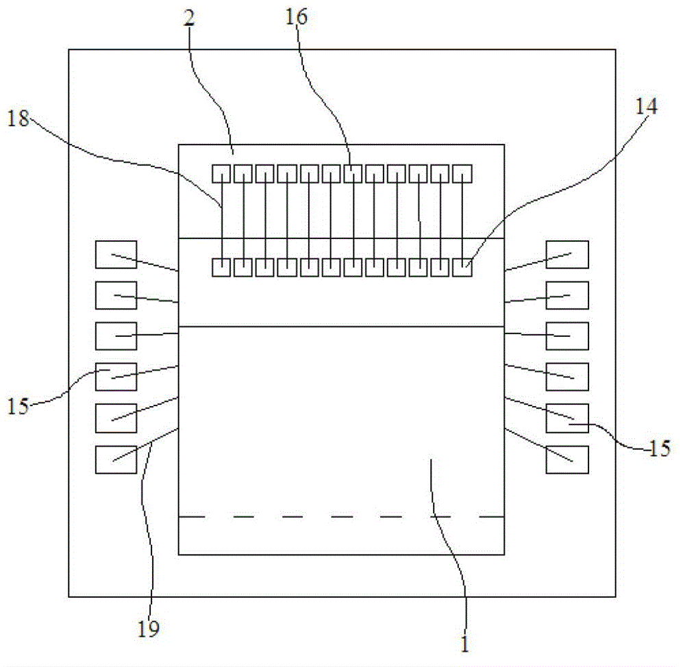
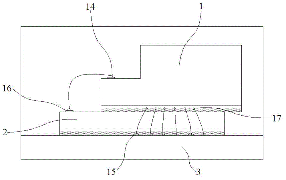
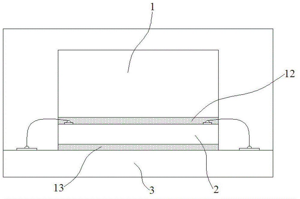
[0032] Embodiment: a capacitive MEMS acceleration sensor, comprising a MEMS acceleration chip 1, a signal processing chip 2 and a substrate 3 for filtering interference signals and processing induction signals, the MEMS acceleration chip 1 is composed of a cover body 4, a micromechanical system 5 and a circuit substrate 6 for generating induction signals, the micromechanical system 5 is composed of an X-axis acceleration sensing area 7, a Y-axis acceleration sensing area 8, and a Z-axis acceleration sensing area 9 for sensing external Z-axis motion, the said The cover body 4 and the circuit substrate 6 are bonded by a sealant layer 10 to form a sealed cavity 11. The micromechanical system 5 is located in the sealed cavity 11 and on the upper surface of the circuit substrate 6. The height of the sealed cavity 11 is 45~55μm;

[0033]The X-axis acceleration sensing area 7 includes an X-direction "H"-shaped moving piece 71 with two through holes, two X-direction moving electrodes ...


PUM


Abstract

A capacitive MEMS acceleration sensor comprising an MEMS acceleration chip (1), a signal processing chip (2) and a substrate (3). The MEMS acceleration chip (1) comprises a cover body (4), a micromechanical system (5) and a circuit substrate (6), the micromechanical system (5) is composed of an X-axis acceleration induction area (7), a Y-axis acceleration induction area (8) and a Z-axis acceleration induction area (9); the Y-axis acceleration induction area (8) comprises a Y-direction 'H'-shaped moving sheet (81) with two through holes, two Y-direction moving electrodes (82) and two Y-direction fixed electrodes (83); the Z-axis acceleration induction area (9) comprises a mass block (24) and a supporting shaft (25) for supporting the center of the mass block (24); the lower surface of the circuit substrate (6) is bonded with a partial area on the upper surface of the signal processing chip (2) through a first insulation adhesive layer (12); the upper surface of the circuit substrate (6) is provided with a plurality of chip welding points (14), the upper surface of the substrate (3) is provided with a plurality of substrate welding points (15) which are distributed in the edge areas on the two sides of the substrate (3), and the upper surface of the signal processing chip (2) is provided with signal input welding points (16) and signal output welding points (17) respectively. The capacitive MEMS acceleration sensor improves the reliability of a device and effectively reduces stress damage to the chips by an external force.

Description

technical field [0001] The invention relates to the technical field of acceleration sensors, in particular to a capacitive MEMS acceleration sensor. Background technique [0002] MEMS acceleration sensors have attracted much attention due to their small size, light weight, low cost, and high reliability, especially in the fields of aerospace and weapon science, which have high requirements for the volume, quality, and reliability of devices. Application prospects. The research on acceleration sensors has developed rapidly in recent years, and high-range acceleration sensors with various performances and ranges have been reported one after another. However, the accelerometer has high requirements for high overload resistance and natural frequency. Usually, the high overload resistance is required to withstand hundreds of thousands of range impact loads, and the natural frequency is required to be as high as tens of kHz, or even hundreds of kHz. Therefore, in applications, M...

Claims


Application Information

Patent Timeline
Patent Type & Authority Patents(China)
IPC IPC(8): G01P15/125
CPCG01P15/125G01P15/18G01P2015/0831
Inventor 陈学峰钟利强杨小平
Owner MIRAMEMS SENSING TECH CO LTD
Learn More