Anti-electromagnetic-interference circuit board

An anti-electromagnetic interference and circuit board technology, which is applied to printed circuit components, electrical components, magnetic field/electric field shielding, etc., can solve the problems of increasing circuit board stacking, increasing costs, and unsatisfactory effects, so as to reduce electromagnetic interference, Mutual interference reduction effect

Active Publication Date: 2013-11-27
GUANGDONG VTRON TECH CO LTD
View PDF5 Cites 5 Cited by
  • Summary
  • Abstract
  • Description
  • Claims
  • Application Information

AI Technical Summary

Problems solved by technology

However, in practical applications, this solution will increase the stacking of circuit boards, thereby increasing the cost. Sometimes the effect is not ideal, and sometimes the interference cannot be completely eliminated, and the ability to resist electromagnetic interference is unstable.

Method used


Image

  • Anti-electromagnetic-interference circuit board
  • Anti-electromagnetic-interference circuit board

Examples


Embodiment 1

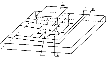
[0020] Such as figure 1 As shown, an anti-electromagnetic interference circuit board includes a circuit board 2 provided with an inductor 1, a mechanical hole 3 is provided in the area where the inductor 1 is installed on the circuit board 2, and the power plane and the ground plane in the circuit board 2 and / or interconnection lines all avoid mechanical holes 3 .

[0021] In this embodiment, aiming at the electromagnetic interference problem of the inductor 1 in the circuit board 2, a mechanical hole 3 is provided in the area where the inductor 1 is installed on the circuit board 2, wherein the mechanical hole 3 penetrates the entire circuit board 2, that is to say, The mechanical hole 3 passes through the power plane and the ground plane on the circuit board 2. Therefore, the position opposite to the mechanical hole 3 on the power plane and the ground plane is empty, and the power plane, the ground plane and / or the power plane on the circuit board 2 The interconnection line...

Embodiment 2

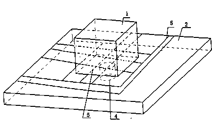
[0026] Such as figure 2 As shown, an anti-electromagnetic interference circuit board includes a circuit board 2 provided with an inductor 1, and the area where the inductor 1 is installed on the circuit board 2 is provided with a forbidden area 4, and the power plane and ground in the circuit board 2 The planes and / or interconnection lines avoid the forbidden area 4 .

[0027] Wherein, the area where the inductor 1 is installed on the circuit board 2 corresponds to all layers of the circuit board 2, that is to say, each layer of the circuit board 2 is provided with a prohibition on the position of the area where the inductor 1 is installed. Layout area 4, so, on the power plane on the circuit board 2, ground plane also is provided with forbidden area, makes power plane, ground plane and / or the interconnection line between each device in the circuit board 2 all avoids this forbidden area. Layout area 4, so that the power plane in the circuit board 2, the ground plane and / or v...

Embodiment 3

[0031] Since the mechanical holes set on the circuit board need to consider the installation requirements and anti-interference requirements of the inductor, when the mechanical holes set on the circuit board are too large, it will affect the installation of the inductor, but if the mechanical holes are too small, the area on the circuit board that avoids the electromagnetic field will be If less, the anti-interference effect will be reduced. Therefore, different from Embodiment 1, this embodiment sets the mechanical hole in the area where the inductor is installed on the circuit board and also sets the forbidden area, so that sufficient mechanical holes can be reserved during the design of the mechanical hole. There is space for the inductor to be installed, and it can be combined with the prohibited area to form an electromagnetic avoidance area to ensure the effect of anti-interference. Preferably, the range of the forbidden area is equal to or larger than the hole area of ​...


PUM


Abstract

The invention relates to the field of circuit boards, in particular to an anti-electromagnetic-interference circuit board. The anti-electromagnetic-interference circuit board comprises a circuit board body provided with an inductor. The area, where the inductor is installed, of the circuit board body is provided with a mechanical hole and / or an arrangement-forbidding area. The power source plane, the ground plane and interconnecting wires in the circuit board body all keep away from the mechanical hole and / or the arrangement-forbidding area. The inductor is a main source of the electromagnetic interference problem in the circuit board body. According to the anti-electromagnetic-interference circuit board, the area, where the inductor is installed, of the circuit board body is provided with the mechanical hole and / or the arrangement-forbidding area, the power source plane and the ground plane in the circuit board body and the interconnecting wires among various parts in the circuit board body all keep away from the mechanical hole and / or the arrangement-forbidding area, therefore, mutual interference between the electromagnetic field generated by the inductor and the electromagnetic fields generated by the areas, intersected with the area where the inductor is installed, of the power source plane, the ground plane and / or the interconnecting wires is avoided, the electromagnetic interference in the circuit board body can be effectively reduced, and the signal quality of the power source plane, the ground plane and the interconnecting wires among the various parts in the circuit board body is improved.

Description

technical field [0001] The present invention relates to the field of circuit boards, more specifically, to a circuit board resistant to electromagnetic interference. Background technique [0002] As the electronic components and traces in the circuit board become denser, the electromagnetic interference in the circuit board becomes very serious. In order to isolate the electromagnetic field, the existing technical solution is that the main circuit board is vertically plugged on the terminal interface board, and a flat transformer with low magnetic flux leakage and low disturbance is used as the signal isolation component. The main circuit board includes signal There are three parts: input, signal output and power supply module. The three parts are isolated by moats, and the moats are uninterrupted until they reach the terminal interface board. In the practical application of this method, the three parts on the main circuit board need to be provided with moats, and the size ...

Claims


Application Information

Patent Timeline
Patent Type & Authority Applications(China)
IPC IPC(8): H05K1/02H05K9/00
Inventor 陈文星褚平由
Owner GUANGDONG VTRON TECH CO LTD
Why Eureka
Try Eureka