
Luminous unit and luminous module thereof

A light-emitting unit and light-emitting module technology, which is applied in the direction of electrical components, lighting and heating equipment, circuits, etc., can solve the problems of high cost, achieve the effects of improving heat conduction efficiency, simplifying assembly, and improving luminous efficiency

Active Publication Date: 2013-12-04
XIAMEN SANAN OPTOELECTRONICS CO LTD
View PDF7 Cites 0 Cited by
  • Summary
  • Abstract
  • Description
  • Claims
  • Application Information

AI Technical Summary

Problems solved by technology

However, flip-chip LEDs are bonded to the substrate by die bonding, and the maximum PN electrodes to be bonded can only be the same size as the LED grain. Therefore, high-precision die-bonding machines are required for die bonding, and the cost required expensive

Method used


Image

  • Luminous unit and luminous module thereof
  • Luminous unit and luminous module thereof
  • Luminous unit and luminous module thereof

Examples


Embodiment Construction

[0068] A light emitting unit and a light emitting module thereof according to preferred embodiments of the present invention will be described below with reference to related drawings, wherein the same elements will be described with the same reference symbols.

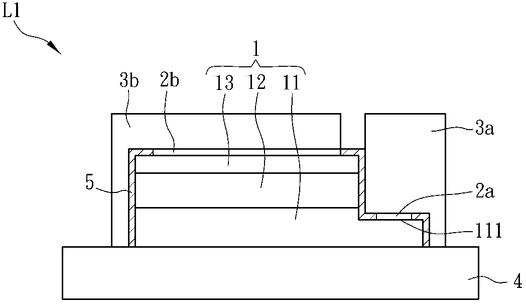
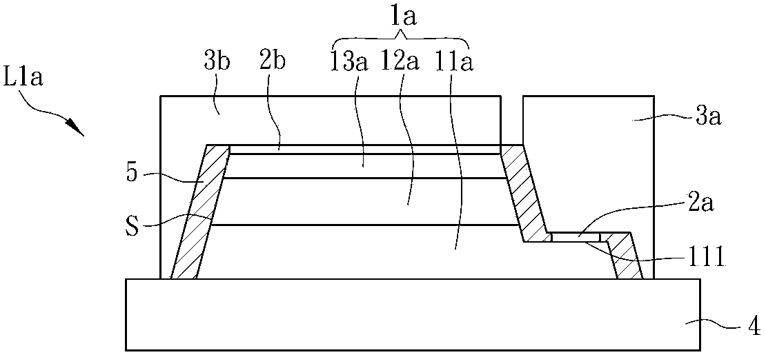
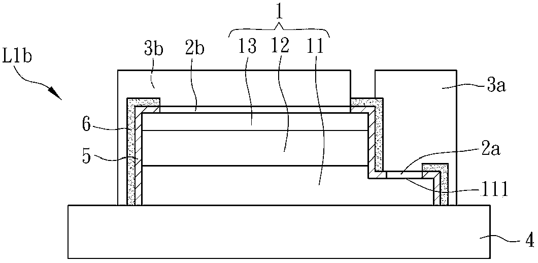
[0069] figure 1 It is a schematic cross-sectional view of a light emitting unit L1 according to the first preferred embodiment of the present invention. Such as figure 1 As shown, the light emitting unit L1 includes an epitaxial stack 1, at least one first electrode 2a, at least one second electrode 2b, a first bonding pad 3a and a second bonding pad 3b. Here, the light emitting unit L1 uses a light emitting diode as its light source.

[0070] The epitaxial stack 1 sequentially includes a first semiconductor layer 11, a light emitting layer 12 and a second semiconductor layer 13, by etching the light emitting layer 12 and the second semiconductor layer 13 to expose part of the first semiconductor layer 11, which can...


PUM


Abstract

The invention discloses a luminous unit. The luminous unit comprises an epitaxial lamination layer, at least a first electrode, at least a second electrode, a first joint sheet and a second joint sheet. The epitaxial lamination layer sequentially comprises a first semiconductor layer, a luminous layer and a second semiconductor layer; the first semiconductor layer is provided with an exposing portion which exposes the second semiconductor layer and the luminous layer; the first electrode is arranged at the exposing portion; the second electrode is arranged at the second semiconductor layer; the first joint sheet is connected with the first electrode; and the second joint sheet is connected with the second electrode. The invention also discloses two luminous units with different structures and a luminous module applying the luminous units.

Description

technical field [0001] The invention relates to a light-emitting unit and a light-emitting module thereof, in particular to an LED light-emitting unit and a light-emitting module without wiring. Background technique [0002] The purpose of light emitting diode (Light Emitting Diode, hereinafter referred to as LED) packaging is to ensure that the LED chip is electrically connected correctly, and to protect the LED chip from being affected by various external factors such as machinery, heat, and humidity. The current LED packaging has diversified packaging forms according to different application occasions, different product shapes and sizes, heat dissipation schemes, and luminous effects. [0003] The existing LED packaging technology requires a package to carry the LED die, but due to the low thermal conductivity of the package and the inconsistent thermal expansion coefficients of the LED die and the package, the components are easily damaged in a high temperature environme...

Claims


Application Information

Patent Timeline
IPC IPC(8): H01L33/62F21V23/00
Inventor 林立凡陈世鹏廖文甲薛清全
Owner XIAMEN SANAN OPTOELECTRONICS CO LTD
Features
  • Generate Ideas
  • Intellectual Property
  • Life Sciences
  • Materials
  • Tech Scout
  • Unparalleled Data Quality
  • Higher Quality Content
  • 60% Fewer Hallucinations
Learn More