PCB board moulding processing method and laminated plate
A PCB board and forming processing technology, applied in the direction of printed circuit, electrical components, printed circuit manufacturing, etc., can solve the problems of increasing product processing cost, difficulty in mass production, poor processing effect, etc., to achieve reduced processing cost, easy operation, Guaranteed quality effect
- Summary
- Abstract
- Description
- Claims
- Application Information
AI Technical Summary
Problems solved by technology
Method used
Image

Examples
Embodiment 1
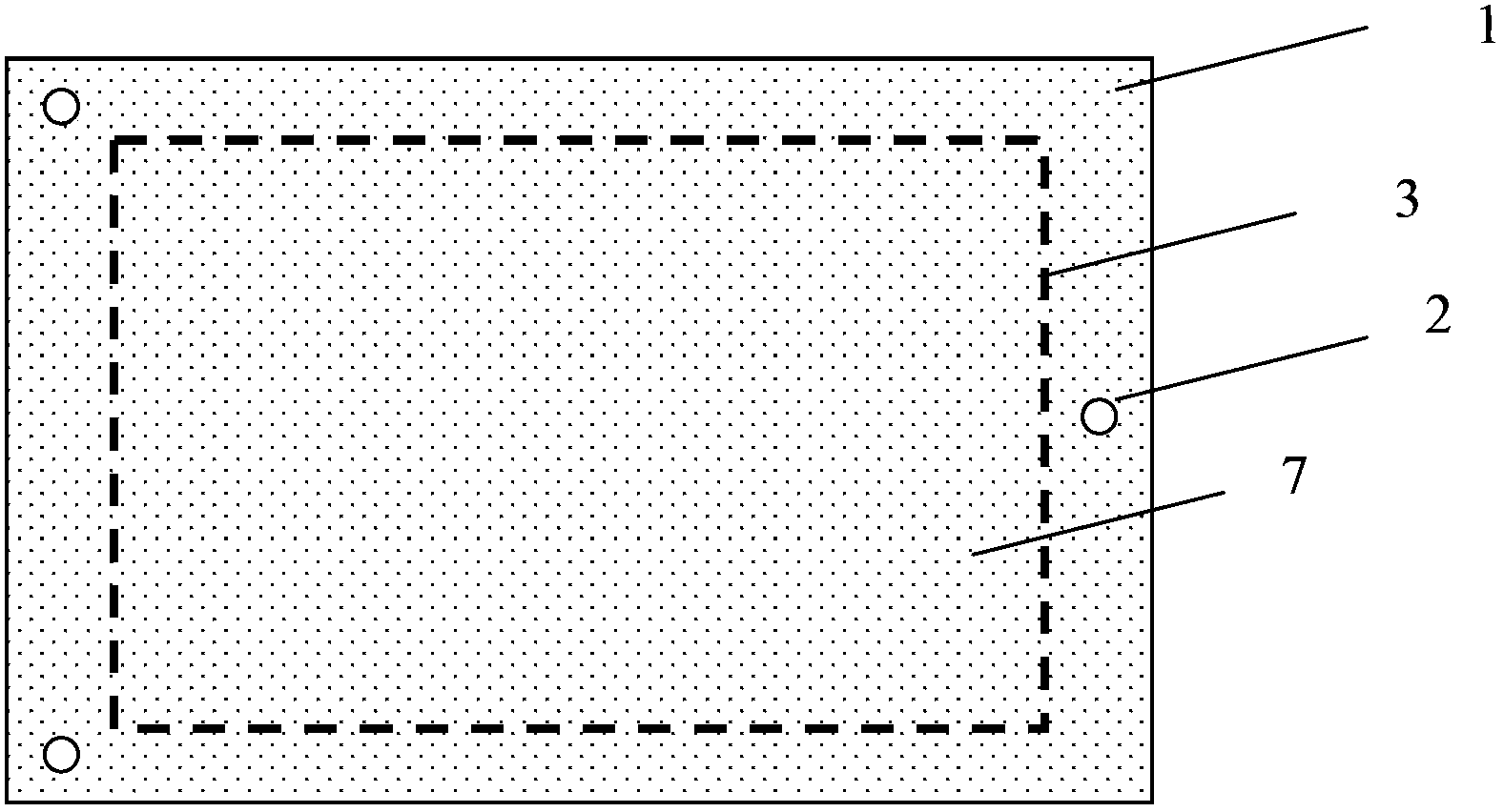
[0040] The PCB board to be formed includes an effective area and an edge area. The effective area contains at least one forming area. The forming process of the PCB is to remove the non-forming area on the PCB to be formed, leaving only the forming area.
[0041] In this embodiment, the effective area only includes one molding area 7 (ie image 3 The area on the PCB board to be formed corresponding to the forming circuit 3 on the middle support plate), that is, the range of the effective area completely overlaps with the range of the forming area. The forming line 3 here is not really set on the support plate, it is actually only preset in the processing program of the milling machine, image 3 The purpose of marking in is to facilitate readers to distinguish the effective area (molding area) and edge area of the PCB board to be formed.
[0042] In this embodiment, the PCB board 1 to be formed adopts a high-frequency high-speed FPC board, that is, a flexible printed circuit...
Embodiment 2
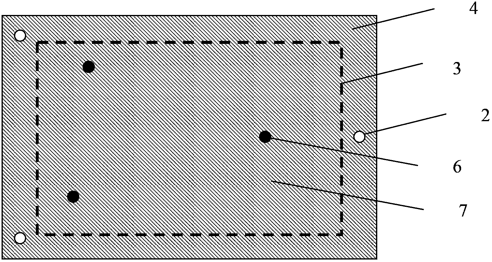
[0062] The difference between this embodiment and Embodiment 1 is that the effective area of the PCB board to be formed includes N molding areas 7, that is, in the laminated board formed after the support plate and the PCB board to be formed are laminated, as Figure 4 As shown, the N molding regions 7 in the laminated board will form N small unit PCBs correspondingly after molding.
[0063] In this embodiment, a positioning unit is provided on the formed laminated board. The positioning unit includes a first positioning unit and N second positioning units.
[0064] The structure and opening position of the first positioning unit are exactly the same as those in Embodiment 1, and will not be described in detail here.
[0065] In this embodiment, among the N forming areas 7 in the laminated board, each forming area 7 is provided with a second positioning unit. The second positioning unit in each molding area 7 includes the second positioning hole 6 arranged in the molding a...
Embodiment 3
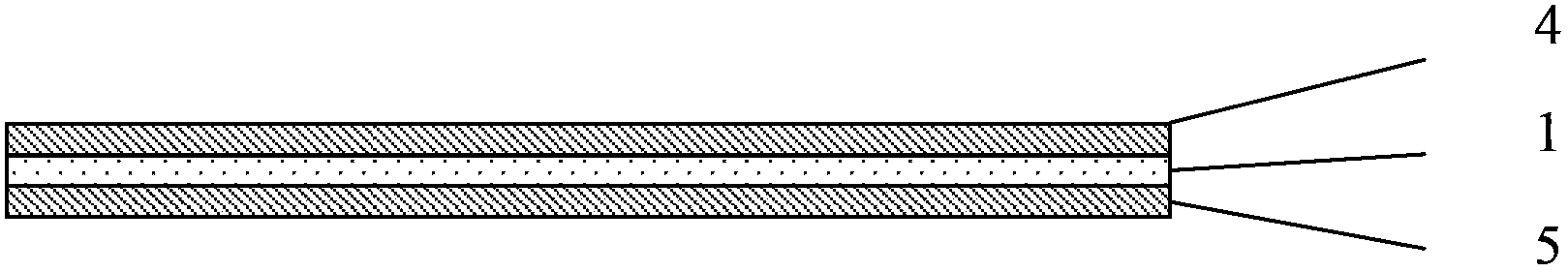
[0069] The difference between this embodiment and Embodiment 1 is that only one support plate is used in this embodiment, that is, only the first base material plate 4 or the second base material plate 5 is included, that is to say, only the PCB board to be formed 1, a support plate is set on one of the sides.
[0070] The laminated board in this embodiment includes a PCB board to be formed and a supporting board, and the supporting board is laminated on one side of the PCB board to be formed. Wherein, a first positioning hole is opened in the edge area of the PCB board to be formed, and a second positioning hole is opened in its effective area; a first alignment hole is opened on the position corresponding to the first positioning hole on the support plate. A second alignment hole is opened at a position corresponding to the second positioning hole.
[0071] The forming and processing method of the PCB board to be formed in this embodiment is the same as that in Embodiment...
PUM
 Abstract
Description
Claims
Application Information