Automatic locating and testing socket for CMOS camera shooting chip floating carrier plate

A test socket and automatic positioning technology, which is applied in the field of automatic positioning test socket of CMOS camera chip floating carrier board, can solve problems such as chip crushing, mechanical failure, and test efficiency reduction, and achieve convenient use, extended service life, and simple operation Effect

Active Publication Date: 2013-12-11
SUZHOU CHUANGRUI MACHINERY & ELECTRICAL TECH
View PDF6 Cites 11 Cited by
  • Summary
  • Abstract
  • Description
  • Claims
  • Application Information

AI Technical Summary

Problems solved by technology

[0003] At present, most of the CMOS imaging test chip automatic sockets basically use single, 1×4 and 2×2 test mechanisms to meet the requirements of the machine. However, due to the high requirements of the optical CMOS chip on the chip optical center and lens center (The test concentricity does not exceed 0.03mm). The PITCH of the chip solder ball is getting smaller and smaller (up to 0.20mm). At the same time, the repeated positioning accuracy of the automatic test machine is not the same, so many test sockets are designed and processed. We have to take care of one and lose the other, reducing the design standard and processing accuracy of the test socket to meet the design tolerance of the product
In this way, the test of the product cannot meet the test requirements to a large extent, which reduces the test pass rate of the product. For example, the image difference adopted by the test system reaches more than 8%, and the misjudgment rate reaches more than 10%. A large number of chips are crushed by the machine during the test process, causing mechanical failures at the same time, resulting in a decrease in test efficiency

Method used


Image

  • Automatic locating and testing socket for CMOS camera shooting chip floating carrier plate

Examples


Embodiment Construction

[0026] The technical solution of the present invention will be further described below in conjunction with the accompanying drawings and a preferred embodiment.

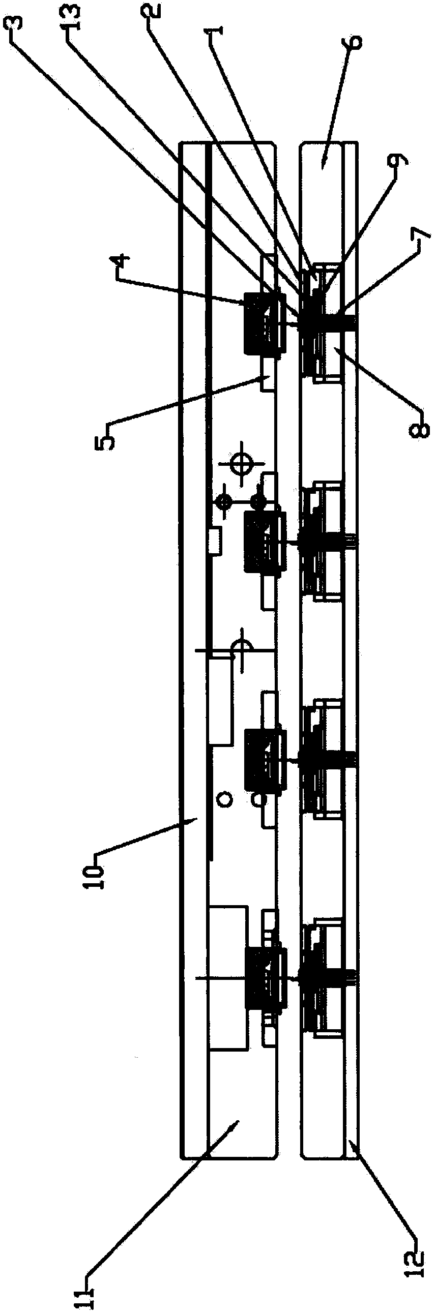
[0027] refer to figure 1 , a kind of CMOS imaging chip floating carrier plate automatic positioning test socket involved in the present embodiment comprises a cooperating upper cover and a base, and the base includes a PCB adapter board 12, a test unit and a floating carrier distributed sequentially from bottom to top. Board 1, the upper cover includes a test lens 4 and a lens pressure plate 5, a light source (such as an LED light board 10) is arranged in the dark room ahead of the test lens, and a contrast is also provided between the test lens and the light source. In the image, the test unit includes a plurality of test probes 7 and a probe holding body 9 for installing the test probes, a probe holding plate 8 and a probe holding frame 11 .

[0028] Further, when the upper cover and the base are closed, the float...


PUM


Abstract

The invention discloses an automatic locating and testing socket for a CMOS camera shooting chip floating carrier plate. The automatic locating and testing socket comprises an upper cover and a base which are mutually matched. A PCB pinboard, a testing unit and the floating carrier plate are sequentially distributed on the base from bottom to top. The upper cover comprises a testing camera lens and a camera lens pressing plate, wherein a light source is arranged in a dark room in front of the testing camera lens, and a comparison image is positioned between the testing camera lens and the light source. The testing unit comprises a plurality of testing probes, a testing probe retention main body, a probe retention plate and a probe retention frame, wherein the testing probe retention main body, the probe retention plate and the probe retention frame are used for installing the testing probes. Furthermore, when the upper cover and the base are buckled, the floating carrier plate is in contact with the camera lens pressing plate, and the floating carrier plate is pushed by the camera lens pressing plate to move downwards. Meanwhile, the floating carrier plate is at least connected with an elastic element which is used for providing force driving the floating carrier plate to move upwards. The automatic locating and testing socket is suitable for different testing machines, can test CMOS chips automatically, efficiently and accurately and is not prone to damaging the CMOS chips.

Description

technical field [0001] The invention relates to a CMOS chip testing device, in particular to a CMOS camera chip floating carrier plate automatic positioning test socket. Background technique [0002] CMOS wafers are photosensitive chip devices formed by processing photosensitive integrated circuits on silicon wafers, which are widely used in mobile phones, computers, camera devices and other equipment. Generally speaking, CMOS wafers have the characteristics of high product circuit integration and small step distance (about 0.2mm) between solder balls used for circuit derivation. [0003] At present, most of the CMOS imaging test chip automatic sockets basically use single, 1×4 and 2×2 test mechanisms to meet the requirements of the machine. However, due to the high requirements of the optical CMOS chip on the chip optical center and lens center (The test concentricity does not exceed 0.03mm). The PITCH of the chip solder ball is getting smaller and smaller (up to 0.20mm). ...

Claims


Application Information

Patent Timeline
Patent Type & Authority Applications(China)
IPC IPC(8): G01R1/04G01R31/26
Inventor 朱小刚柳慧敏
Owner SUZHOU CHUANGRUI MACHINERY & ELECTRICAL TECH
Why Eureka
Try Eureka