Wafer Dicing Method

A cutting method and wafer technology, applied in electrical components, semiconductor/solid-state device manufacturing, circuits, etc., can solve the problems of wafer cracking, wafer warpage, and delamination between metal layers, etc., to improve cutting and cracking. Effect

Active Publication Date: 2016-06-22
北京中科微知识产权服务有限公司
View PDF4 Cites 0 Cited by
  • Summary
  • Abstract
  • Description
  • Claims
  • Application Information

AI Technical Summary

Problems solved by technology

However, when ultra-thin wafers are processed using traditional processes, the wafers are prone to warping after grinding, and wafer cracks are likely to occur during subsequent processing operations; delamination between metal layers

Method used


Image

  • Wafer Dicing Method
  • Wafer Dicing Method
  • Wafer Dicing Method

Examples


Embodiment Construction

[0018] In order to make the above objectives, features and advantages of the present invention more obvious and understandable, the present invention will be further described in detail below with reference to the accompanying drawings and specific embodiments.

[0019] The "one embodiment" or "embodiment" referred to herein refers to a specific feature, structure, or characteristic that can be included in at least one implementation of the present invention. The appearances of "in one embodiment" in different places in this specification do not all refer to the same embodiment, nor are they separate or selectively mutually exclusive embodiments with other embodiments.

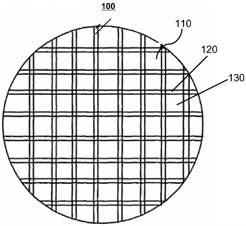
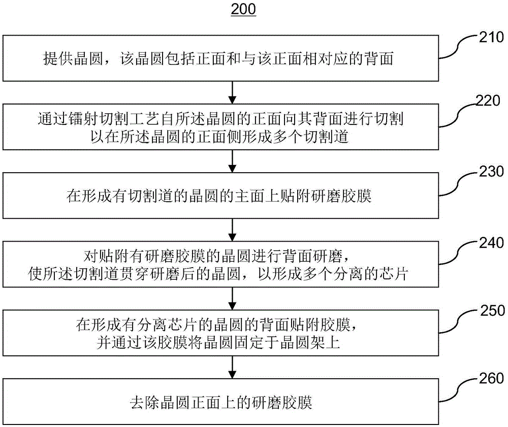
[0020] In the wafer cutting method of the present invention, a plurality of cutting channels are formed on the front side of the wafer by laser cutting, and then the back side of the wafer is thinned by a grinding process, thereby forming a plurality of separated chips. Since laser cutting and grinding processes ar...


PUM


Abstract

The invention provides a wafer cutting method. The wafer cutting method includes the steps that a wafer is provided, wherein the wafer comprises a front face and a back face corresponding to the front face; cutting is conducted from the front face of the wafer to the back face of the wafer through a laser cutting technology so that a plurality of cutting channels can be formed in the front face of the wafer; a grinding adhesive film is attached to the front face with the formed cutting channels of the wafer; back face grinding is conducted on the wafer which is provided with the grinding adhesive film in an attaching mode, the cutting channels are made to penetrate through the ground wafer, and therefore a plurality of separated chips can be formed. Due to the facts that laser cutting is used first, then the grinding process is adopted, and laser cutting can not generate cutting stress, the wafer cutting method not only can avoid rupture of thin wafers but also can be applied to cutting wafers with low dielectric constants.

Description

【Technical Field】 [0001] The present invention relates to the technical field of semiconductor manufacturing, in particular to a wafer cutting method. 【Background technique】 [0002] In the semiconductor manufacturing process, it is necessary to cut the wafer into individual dies, and then make these chips into different semiconductor packaging structures. Please refer to figure 1 As shown, it is a top view of a wafer 100. The wafer 100 includes a front surface 110 and a back surface corresponding to the front surface 110, wherein a plurality of longitudinal and transverse cutting streets 120 are provided on the front surface 110 to define a plurality of chips in the wafer 100 130. Wherein, the front surface 110 of the wafer 100 refers to the surface on which the components, stacks, interconnect lines, and bonding pads are formed on the semiconductor substrate. [0003] The wafer dicing method in the prior art usually includes: first using a grinding wheel of a grinder to backsi...

Claims


Application Information

Patent Timeline
Patent Type & Authority Patents(China)
IPC IPC(8): H01L21/78
Inventor 陆建刚
Owner 北京中科微知识产权服务有限公司
Why Eureka
Try Eureka