Integrated packaging structure of surface acoustic wave filter and packaging method thereof

A surface acoustic wave, integrated packaging technology, applied in electrical components, impedance networks, etc., can solve the problems of adverse effects on the overall performance of the surface acoustic wave filter application system, complex interconnection structure, poor anti-interference ability, etc., to improve Overall performance, easy synchronization, strong anti-interference ability

Inactive Publication Date: 2013-12-11
YANGZHOU UNIV
View PDF4 Cites 8 Cited by
  • Summary
  • Abstract
  • Description
  • Claims
  • Application Information

AI Technical Summary

Problems solved by technology

[0003] The purpose of the present invention is to overcome above-mentioned deficiencies in the prior art, overcome the surface acoustic wave filter chip and the matching tuner circuit in the prior art to separate inside and outside the package, the interconnection wire structure is complex, the loss is large, and the anti-interference ability is poor, and then The shortcomings that have a significant adverse effect on the overall performance of the surface acoustic wave filter application system, thereby providing an integrated packaging structure and packaging method for the surface acoustic wave filter

Method used


Image

  • Integrated packaging structure of surface acoustic wave filter and packaging method thereof
  • Integrated packaging structure of surface acoustic wave filter and packaging method thereof
  • Integrated packaging structure of surface acoustic wave filter and packaging method thereof

Examples


Embodiment 1

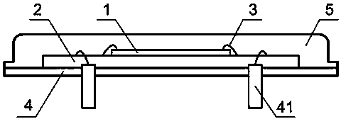
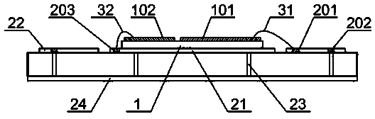
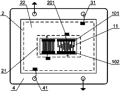
[0022] The surface acoustic wave filter integrated packaging structure includes a surface acoustic wave filter chip 1, a matching tuning circuit 22 electrically connected to the surface acoustic wave filter chip, and a package shell, the package shell is composed of a package base 4 and an outer pin 41 of the package base 1. The sealing cap 5 is formed, and the sealing cap is covered on the packaging base.

[0023] A tuning substrate 2 is provided, and the tuning substrate is arranged in the package shell. The tuning substrate is a high-frequency double-sided printed circuit board. A large-area grounded metal film 24 is provided on the back.

[0024] The matching tuning circuit 22 is fabricated on the tuning substrate, and the surface acoustic wave filter chip is glued on the chip bonding area. The bonding wires include signal bonding wires 31 and grounding bonding wires 32, and the signal bonding wires are sequentially connected to the signal electrodes 101 of the surface ac...

Embodiment 2

[0034] This embodiment is an integrated package of a single surface acoustic wave filter chip and a matching tuning circuit for a single channel filter.

[0035] The surface acoustic wave filter integrated packaging structure includes a single surface acoustic wave filter chip 11, a single channel filter matching and tuning circuit 22 electrically connected to the single surface acoustic wave filter chip, and a packaging shell. The packaging shell is composed of a packaging base 4, outer pins 41 of the packaging base, and a sealing cap 5, and the sealing cap covers the packaging base.

[0036] A tuning substrate 2 is provided, the middle area of ​​the front is a chip bonding area 21, a single-channel filter matching tuning circuit 22 is provided in the peripheral area of ​​the front, a large-area grounded metal film 24 is provided on the back, and the tuning substrate 2 is arranged in the packaging shell , the single-channel filter matching tuning circuit 22 is arranged on the...

Embodiment 3

[0048] This embodiment is an integrated packaging of a monolithic surface acoustic wave filter group chip and a multi-channel filter matching and tuning circuit.

[0049] The surface acoustic wave filter integrated packaging structure includes a monolithic integrated surface acoustic wave filter group chip 12, a multi-channel filter matching and tuning circuit 22 electrically connected to the surface acoustic wave filter chip, and a packaging shell. The packaging shell is composed of a packaging base 4, outer pins 41 of the packaging base, and a sealing cap 5, and the sealing cap covers the packaging base.

[0050] A tuning substrate 2 is provided, the middle area of ​​the front is a chip bonding area 21, a multi-channel filter matching tuning circuit 22 is provided in the peripheral area of ​​the front, a large-area grounded metal film 24 is provided on the back, and the tuning substrate 2 is arranged in the packaging shell , the multi-channel filter matching and tuning circu...


PUM


Abstract

The invention discloses an integrated packaging structure of a surface acoustic wave filter and a packaging method thereof and belongs to the technical field of surface acoustic waves. The integrated packaging structure comprises a surface acoustic wave filter chip, a matching tuned circuit and a packaging shell. The packaging shell is composed of a packaging base, outer pins of the packaging base, and a sealing cap. The sealing cap covers the packaging base. The integrated packaging structure is characterized in that a tuned substrate is arranged, the matching tuned circuit is manufactured on the tuned substrate, the surface acoustic wave filter chip is adhered to the tuned substrate and is electrically connected with the matching tuned circuit through a bonding wire, and the tuned substrate is adhered to the packaging base and is electrically connected with the outer pins of the packaging base through bonding wires. According to the integrated packaging structure, the surface acoustic wave filter chip and the matching tuned circuit are integrated and packaged in the same packaging body, so that mutual connection structures between the surface acoustic wave filter chip and an application circuit, and between the matching tuned circuit and an application circuit are simplified. Consequently, the integrated packaging structure has the advantages of being compact in structure, small in consumption, strong in antijamming capability, and the like, and helps to improve the overall performance of an application system of a surface acoustic wave filter.

Description

technical field [0001] The invention relates to an electronic packaging structure and packaging method, in particular to an integrated packaging structure and packaging method of a surface acoustic wave filter, belonging to the technical field of surface acoustic wave. Background technique [0002] When the surface acoustic wave filter is connected to the application circuit, it is often necessary to set a tuning circuit between it and the front and rear circuits to achieve the matching of the electrical parameters between the device and the front and rear circuits, so as to exert the best performance of the surface acoustic wave filter. performance. The surface acoustic wave filter in the prior art generally adopts an independent packaging method, that is, each filter chip is placed in a package shell separately, and the matching tuning circuit is arranged outside the device package. The disadvantages brought about by this are The structure of the interconnection between t...

Claims


Application Information

Patent Timeline
Patent Type & Authority Applications(China)
IPC IPC(8): H03H9/64H03H9/05H03H9/02
Inventor 赵成陈磊胡经国
Owner YANGZHOU UNIV
Why Eureka
Try Eureka