Schottky diode for rectifying circuit and rectifying circuit
A Schottky diode and rectifier circuit technology, applied in the field of wireless transmission, can solve the problems of component packaging structure, complex interconnection, complex Schottky diode device structure, etc.
- Summary
- Abstract
- Description
- Claims
- Application Information
AI Technical Summary
Problems solved by technology
Method used
Image
Examples
Embodiment 1
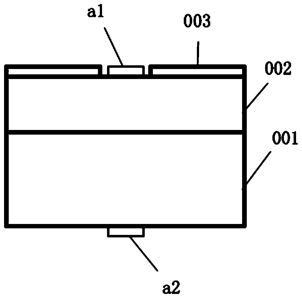
[0025] See figure 1 , figure 1 A schematic structural diagram of a Schottky diode used in a rectifier circuit provided by an embodiment of the present invention. The Schottky diode used in the rectifier circuit includes: a substrate layer 001, a Ge layer 002, a compressive stress layer 003, a first metal electrode a1, and a second metal electrode a2, wherein,
[0026] The Ge layer 002 and the compressive stress layer 003 are sequentially stacked on the first surface of the substrate layer 001, the compressive stress layer 003 is provided with electrode holes, and the first metal electrode a1 is provided on the Ge layer 002 and disposed in the electrode hole, the second metal electrode a2 is disposed on the second surface of the substrate layer 001 opposite to the first surface.
[0027] The beneficial effects of the present invention are:
[0028] 1. The present invention designs the material of the Schottky diode, adopts the strained Ge layer as the semiconductor layer of ...
Embodiment 2
[0032] see again figure 1 , this embodiment focuses on the detailed description of the Schottky diode used in the rectifier circuit on the basis of the above embodiments. Specifically, the Schottky diode includes:
[0033] Including: a substrate layer 001, a Ge layer 002, a compressive stress layer 003, a first metal electrode a1, and a second metal electrode a2, wherein,
[0034] The Ge layer 002 and the compressive stress layer 003 are sequentially stacked on the first surface of the substrate layer 001, the compressive stress layer 003 is provided with electrode holes, and the first metal electrode a1 is provided on the Ge layer 002, the second metal electrode a2 is disposed on the second surface of the substrate layer 001 opposite to the first surface.
[0035] Wherein, the substrate layer 001 is a germanium substrate layer, specifically, the N-type doping concentration can be 10 20 cm -3 N-type single crystal germanium (Ge).
[0036] It should be noted that, as a sub...
Embodiment 3
[0067] In this embodiment, on the basis of the above-mentioned embodiments, an embodiment of the present invention provides a rectification circuit, wherein the rectification circuit includes the Schottky diode described in any one of the above-mentioned embodiments.
[0068] Because the rectifier circuit uses a Schottky diode with high electron mobility, it has high energy conversion efficiency. The rectifier circuit can be used in a wireless transmission system and can improve the energy conversion efficiency of the wireless transmission system.
PUM
| Property | Measurement | Unit |
|---|---|---|
| Doping concentration | aaaaa | aaaaa |
| Thickness | aaaaa | aaaaa |
| Doping concentration | aaaaa | aaaaa |
Abstract
Description
Claims
Application Information


