Microstructural plasma device based on printed circuit board process
A technology of printed circuit boards and ionic devices, applied in the direction of plasma, electrical components, etc., to achieve the effect of less process links, easy production and production, and easy production
- Summary
- Abstract
- Description
- Claims
- Application Information
AI Technical Summary
Problems solved by technology
Method used
Image

Examples
Embodiment Construction
[0022] The present invention will be described in further detail below.
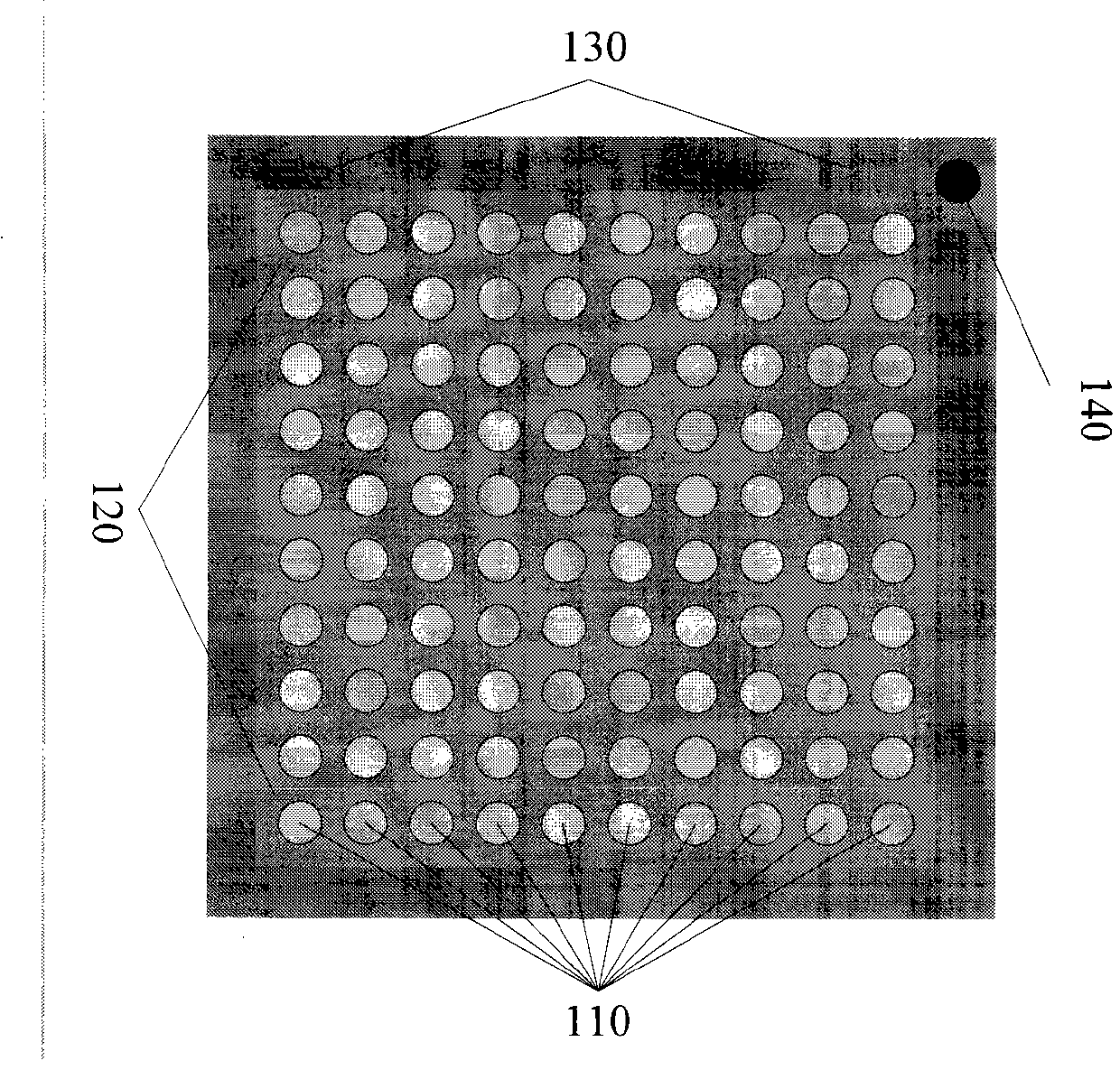
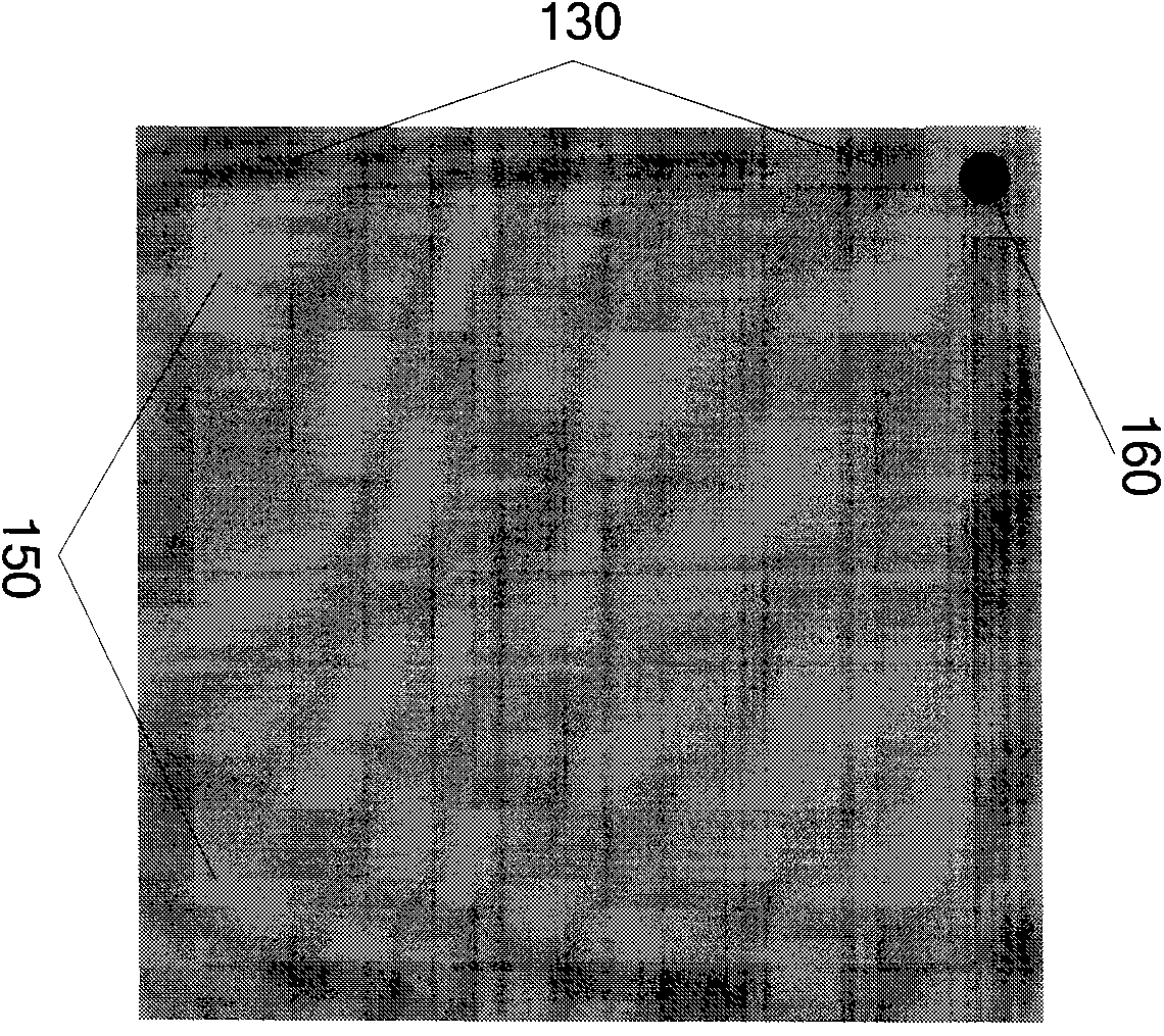
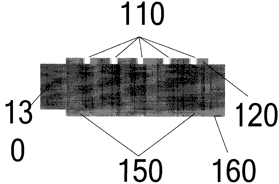
[0023] The microcavity of the device is composed of an upper electrode, an intermediate dielectric layer and a lower electrode, and each unit of the device is driven by the upper and lower electrodes. Based on insulating dielectric epoxy resin material, two layers of copper foil are made on the upper and lower surfaces of the substrate, and a certain safety distance is left between the edge of the copper foil and the edge of the substrate. Cylindrical microcavity half-through holes (just passing through the upper electrode but not through the intermediate dielectric layer and the lower electrode) units are arranged in an array, and the distance between rows in the array is not less than the distance between columns. The upper and lower layers of copper foil separated by the bottom plate are used as the upper and lower electrodes, and the two electrodes are respectively led out to the connecting terminals...
PUM
 Abstract
Description
Claims
Application Information
 - R&D
- Intellectual Property
- Life Sciences
- Materials
- Tech Scout
- Unparalleled Data Quality
- Higher Quality Content
- 60% Fewer Hallucinations
Browse by: Latest US Patents, China's latest patents, Technical Efficacy Thesaurus, Application Domain, Technology Topic, Popular Technical Reports.
© 2025 PatSnap. All rights reserved.Legal|Privacy policy|Modern Slavery Act Transparency Statement|Sitemap|About US| Contact US: help@patsnap.com