Solid electrolytic condenser packaging structure used for reducing equivalent series resistance and production method thereof
A technology of equivalent series resistance and solid-state electrolysis, applied in solid electrolytic capacitors, electrolytic capacitors, capacitors, etc. The effect of crystal strength
- Summary
- Abstract
- Description
- Claims
- Application Information
AI Technical Summary
Problems solved by technology
Method used
Image
Examples
no. 1 example 〕
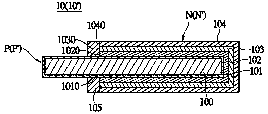
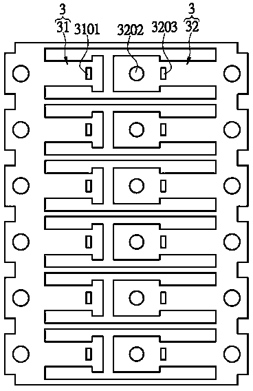
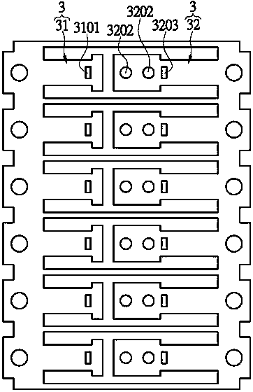
[0063] see Figure 1 to Figure 6 as shown, figure 1 It is a schematic side view sectional view of the first stacked capacitor 10 or the second stacked capacitor 10', Figure 2A is a schematic diagram of the upper side of one of the conductive units 3, Figure 2B is a schematic diagram of the upper side of another conductive unit 3, Figure 2C It is a schematic diagram of the upper side of yet another conductive unit 3, image 3 is a schematic top view of the first stacked capacitor 10 disposed on the conductive unit 3, Figure 4 is a schematic side view of the solid electrolytic capacitor packaging structure Z, Figure 5 for Figure 4 The enlarged schematic diagram of part A in, Image 6 It is a flow chart of the manufacturing method of the package structure Z of the solid electrolytic capacitor. As can be seen from the above drawings, the first embodiment of the present invention provides a solid electrolytic capacitor packaging structure Z for reducing the equivalent ...
no. 2 example
[0074] see Figure 7 and Figure 8 as shown, Figure 7 is a schematic side view of the package structure of a solid electrolytic capacitor, and Figure 8 for Figure 7 An enlarged schematic view of part A in Fig. Depend on Figure 7 and Figure 4 comparison of, and Figure 8 and Figure 5 It can be seen from the comparison that the biggest difference between the second embodiment of the present invention and the first embodiment lies in: figure 1 , Figure 7 and Figure 8As shown, in the second embodiment, the capacitor unit 1 includes a plurality of second stacked capacitors 10' that are stacked together in sequence and electrically connected to each other. Wherein, each second stacked capacitor 10' has a second positive part P' and a second negative part N', and the second stacked capacitor 10' at the bottom can be fixed on the second conductive terminal by conductive glue 11. 32 on the lower surface 3201, and the conductive adhesive 11 has a third conductive part...
no. 3 example
[0077] see Figure 9 and Figure 10 as shown, Figure 9 is a schematic top view of the first stacked capacitor disposed on the conductive unit, and Figure 10 It is a schematic side view of the package structure of a solid electrolytic capacitor. Depend on Figure 9 and image 3 comparison of, and Figure 10 and Figure 4 It can be seen from the comparison that the biggest difference between the three embodiments of the present invention and the first embodiment is that: in the third embodiment, the second conductive terminal 32 has an upper surface 3200, a lower surface 3201 corresponding to the upper surface 3200, a The side surface 3204 connected between the upper surface 3200 and the lower surface 3201 , and at least one through slot 3205 connected between the upper surface 3200 , the lower surface 3201 and the side surface 3204 . The bottommost first stacked capacitor 10 can be fixed on the upper surface 3200 of the second conductive terminal 32 through the conduct...
PUM
 Abstract
Description
Claims
Application Information


