OLED array substrate, manufacturing method thereof and display device

A technology of an array substrate and a manufacturing method, which is applied in the display field, can solve the problems of affecting the display effect, and the TFT is easily exposed to light, and achieves the effect of ensuring the display effect.

Active Publication Date: 2013-12-18
BOE TECH GRP CO LTD
View PDF6 Cites 31 Cited by
  • Summary
  • Abstract
  • Description
  • Claims
  • Application Information

AI Technical Summary

Problems solved by technology

[0004] Embodiments of the present invention provide an OLED array substrate and a manufacturing method thereof, as well as a display device provided with the OLED array substrate, which solves the problem that the TFT in the existing active matrix OLED display device is easily exposed to light and affects the display effect. technical problem

Method used


Image

  • OLED array substrate, manufacturing method thereof and display device
  • OLED array substrate, manufacturing method thereof and display device
  • OLED array substrate, manufacturing method thereof and display device

Examples


Embodiment 1

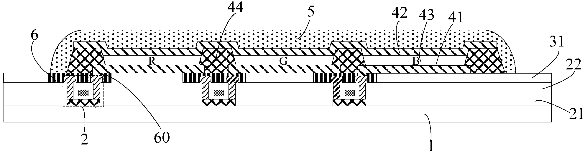
[0049] Such as figure 1 As shown, the OLED array substrate provided by the embodiment of the present invention includes a TFT2 disposed on a base substrate 1 , a gate insulating layer 21 and an interlayer insulating layer 22 , and a first protective layer 31 is disposed above the TFT2. A first electrode 41, a light-emitting layer 43, and a second electrode 42 are sequentially arranged above the first protective layer 31 from bottom to top, wherein the light-emitting layer 43 is a color including three colors of red (R), green (G), and blue (B). luminous layer. The black matrix 6 above the TFT 2 is disposed on the same layer as the first protection layer 31 , and the black matrix 6 is provided with a via hole 60 . The first electrodes 41 are connected to the TFT 2 through via holes 60 , and adjacent first electrodes 41 are separated by barrier walls 44 . In addition, an encapsulation layer 5 is usually provided above the second electrode 42 .

[0050] Preferably, the first e...

Embodiment 2

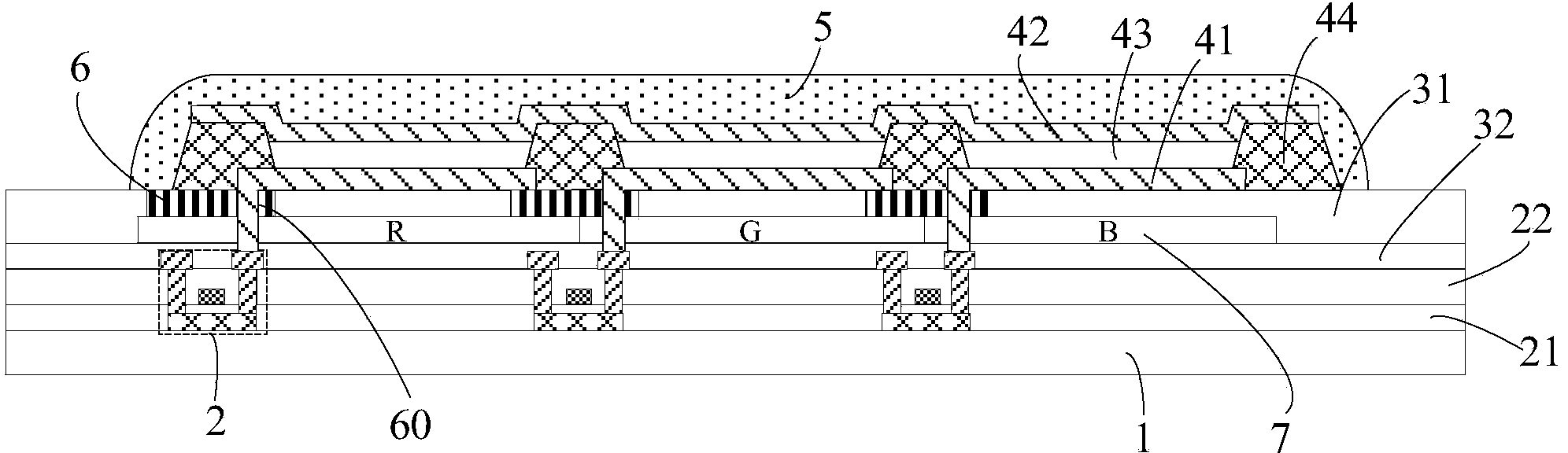
[0063] Such as figure 2 and image 3 As shown, the OLED array substrate provided by the embodiment of the present invention includes a TFT2, a gate insulating layer 21 and an interlayer insulating layer 22 arranged on the base substrate 1, and above the TFT2 are arranged red (R), green (G), The color filter layer 7 of three colors of blue (B), and the first protective layer 31 is arranged on the color filter layer 7 . A first electrode 41 , a light emitting layer 43 , and a second electrode 42 are sequentially disposed above the first protective layer 31 from bottom to top, wherein the light emitting layer 43 is a white light emitting layer. The black matrix 6 above the TFT 2 is disposed on the same layer as the first protection layer 31 , and a via hole 60 penetrating through the black matrix 6 and the color filter layer 7 is opened. The first electrodes 41 are connected to the TFT 2 through via holes 60 , and adjacent first electrodes 41 are separated by barrier walls 44 ...

Embodiment 3

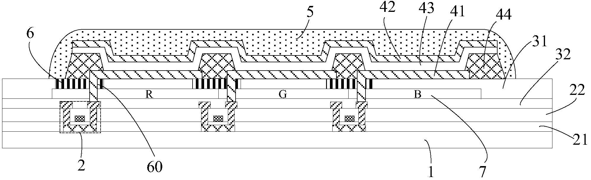
[0082] The embodiment of the present invention is basically the same as embodiment 2, the difference is that, as Figure 4 and Figure 5 As shown, in this embodiment, the black matrix 6 and the color filter layer 7 are arranged in the same layer, and the via hole 60 penetrates through the first protection layer 31 , the black matrix 6 and the second protection layer 32 .

[0083] In the OLED array substrate provided by the embodiment of the present invention, a black matrix 6 is arranged above the TFT 2, and the first electrode 41 of the OLED passes through the via hole 60 penetrating the first protective layer 31, the black matrix 6 and the second protective layer 32. Connect with TFT2. During the display process of TFT2 driving the OLED, the black matrix 6 can block the light emitted by the OLED and prevent the TFT2 from being illuminated, so the current in the OLED driven by the TFT2 will not be wrong, thereby ensuring the display of the active matrix OLED display device ...


PUM


Abstract

The embodiment of the invention discloses an OLED array substrate, a manufacturing method of the OLED array substrate and a display device with the OLED array substrate, and belongs to the technical field of display. The OLED array substrate, the manufacturing method of the OLED array substrate and the display device with the OLED array substrate solve the technical problems that a TFT of an existing active matrix type OLED display device is easily illuminated by light, and the display effect is influenced. The OLED array substrate comprises thin film transistors arranged on a substrate, wherein black matrixes are arranged on the thin film transistors, a through hole is formed in each black matrix, first electrodes, a luminous layer and a second electrode are arranged on the tops of the black matrixes in sequence from bottom to top, the first electrodes are connected with the thin film transistors through the through holes, and every two adjacent first electrodes are separated through a blocking wall. The OLED array substrate can be applied to display devices such as OLED panels, television sets, displayers, digital photo frames, mobile phones and tablet personal computers.

Description

technical field [0001] The invention belongs to the field of display technology, and in particular relates to an OLED array substrate, a manufacturing method thereof, and a display device provided with the OLED array substrate. Background technique [0002] Organic Electroluminescence Display (OELD for short), also known as Organic Light-Emitting Diode (OLED for short) display device, has low energy consumption, high brightness, fast response time, wide viewing angle, light weight, etc. Advantages, has recently been widely used in mobile communication terminals, personal digital assistants (PDA), handheld computers and other equipment. OLED display devices are divided into passive matrix type and active matrix type. Among them, active matrix OLED display devices use thin film transistors (Thin Film Transistor, referred to as TFT) to drive OLEDs, which have higher luminous efficiency and better display Effect. [0003] The inventors found in the process of realizing the pre...

Claims


Application Information

Patent Timeline
Patent Type & Authority Applications(China)
IPC IPC(8): H01L27/32H01L51/52H01L51/56
CPCH10K59/123H10K59/126H10K50/865H10K50/844H10K59/38H10K71/00H10K59/1201
Inventor 程鸿飞张玉欣
Owner BOE TECH GRP CO LTD
Why Eureka
Try Eureka