Audio frequency amplifier adjunct circuit used for eliminating emitter output stage

A technology of audio amplifiers and additional circuits, applied in the direction of transducer circuits, sensors, electrical components, etc., can solve the problems of unstable working status of T10 and T11, and achieve the effect of eliminating interference

Active Publication Date: 2013-12-18
胡福生
View PDF3 Cites 4 Cited by
  • Summary
  • Abstract
  • Description
  • Claims
  • Application Information

AI Technical Summary

Problems solved by technology

[0010] It can be seen that the fluctuation of the power supply voltage and the change of the ambient temperature will have an impact on the bias voltages Vb+ and Vb- of T10 and T11 generated by the voltage drop of the collector load resistors Rc+ and Rc- of T7 and T8, causing T10 and T11 to work unstable state

Method used


Image

  • Audio frequency amplifier adjunct circuit used for eliminating emitter output stage
  • Audio frequency amplifier adjunct circuit used for eliminating emitter output stage
  • Audio frequency amplifier adjunct circuit used for eliminating emitter output stage

Examples


Embodiment 1

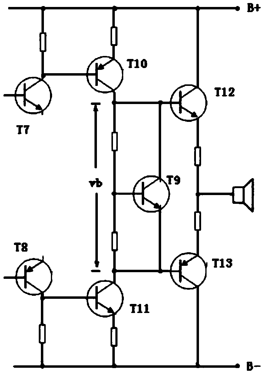
[0043] Such as Figure 4 and Figure 5 As shown, the detection circuit includes a pair of diodes D1, D2 and a group of symmetrical detection PNP transistor T1 and detection NPN transistor T2, the cathode of the diode D1 is connected to the base of the PNP transistor T1, and the diode D2 The anode of the NPN transistor T2 is connected to the base.

[0044]The amplifying circuit then includes a pair of amplifying NPN transistor T3 and amplifying PNP transistor T4 with the function of amplifying the current. In addition, resistors R3 and R4 are connected in series between the emitters of the amplifying transistors T3 and T4 in the amplifying circuit, and the R7, T3, R3, R4, T4 and R8 are sequentially connected in series, and the resistance values ​​of R7 and R8 are equal.

[0045] The adjustable constant current source circuit is composed of a group of symmetrical constant current source PNP transistors T5 and constant current source NPN transistors T6.

[0046] The collector ...

Embodiment 2

[0051] Such as Figure 6 and Figure 7 As shown, the difference between this embodiment and Embodiment 1 is that: the detection circuit includes a diode D and a detection transistor T1 for detection, and the diode D is connected to the base of the detection transistor T1; The amplifying circuit includes an amplifying transistor T3, the adjustable constant current source circuit is composed of a group of symmetrical constant current source PNP transistor T5 and constant current source NPN transistor T6, the constant current source PNP transistor T5 and constant current source NPN The bases of the transistor T6 are respectively connected to two sets of equal-value voltage dividers R7 and R8.

[0052] The amplifying circuit is connected with the adjustable constant current source circuit through an optocoupler OC.

[0053] The specific connection relationship of each circuit is: the collector of the detection transistor T1 is connected to the base of the amplifier transistor T3...

Embodiment 3

[0057] Such as Figure 8 and Figure 9 As shown, this embodiment is a combination and extension of Embodiment 1 and Embodiment 2, wherein the detection circuit uses a pair of diodes D1, D2 and a group of symmetrical detection PNP transistor T1 and detection NPN transistor T2, the diode D1 The negative pole of the diode D2 is connected to the base of the detection PNP transistor T1, and the anode of the diode D2 is connected to the base of the detection NPN transistor T2.

[0058] Correspondingly, the amplifying circuit includes an amplifying NPN transistor T3 and an amplifying PNP transistor T4, and the adjustable constant current source is composed of a constant current source PNP transistor T5 and a constant current source NPN transistor T6, and the constant current source The bases of the PNP transistor T5 and the constant current source NPN transistor T6 are respectively connected to two sets of equal voltage dividers R7, R5 and R6, R8.

[0059] The connection relationsh...


PUM


Abstract

The invention discloses an audio frequency amplifier adjunct circuit used for eliminating an emitter output stage. The audio frequency amplifier adjunct circuit used for eliminating the emitter output stage comprises a detection circuit, an amplifying circuit and an adjustable constant flow source circuit, wherein the detection circuit is composed of a diode and an audion, the diode is connected with the base of the audion, and the diode of the detection circuit generates reference voltage to compare and detect the constitution of the circuit; the amplifying circuit is used for amplifying current signals; the adjustable constant flow source circuit is used for generating adjustable constant flow currents; the detection circuit is connected with the amplifying circuit, and the amplifying circuit is connected with the adjustable constant flow source circuit. The adjunct circuit provides reference voltage and carries out comparison detection, the currents are amplified and then enter the adjustable constant flow source circuit to generate adjustable constant flow currents so that an audio amplifier can be controlled and the work voltage of an output stage of the audio amplifier can keep stable, the emitter output of the amplifying circuit is eliminated, collector output is achieved, and the interference with the output stage of the audio amplifier of a transistor by reactive potential voltage of a loudspeaker is eliminated.

Description

technical field [0001] The invention relates to the field of amplifying circuits of audio amplifiers, in particular to an additional circuit applied to audio amplifier circuits without emitter output stages. Background technique [0002] At present, all audio systems on the market use electric speakers to play sound. According to Lengz's law, the inductance coil of the dynamic speaker will generate a counter electromotive force voltage. The current transistor audio amplifier power output stage adopts the common collector emitter output mode as the mainstream, and the output terminal is connected to the speaker. When the power output stage is in the base At the same time, the emitter is also input with the back electromotive voltage of the speaker. This back electromotive voltage will cause certain interference to the working state of the emitter output stage. [0003] From the three configurations of the transistor amplifier circuit: the common emitter circuit, the common b...

Claims


Application Information

Patent Timeline
IPC IPC(8): H04R3/00
Inventor 胡福生
Owner 胡福生
Why Eureka
Try Eureka