
A fpga embedded independent dual-port bram IP hard core

A dual-port, hard-core technology, applied in the FPGA field, can solve problems such as the asynchronous complexity of internal control signal transmission, achieve the effects of weakened drive capability, optimized circuit power consumption, and reduced mutual pull current

Active Publication Date: 2016-10-26
FUDAN UNIV
View PDF4 Cites 0 Cited by
  • Summary
  • Abstract
  • Description
  • Claims
  • Application Information

AI Technical Summary

Problems solved by technology

For traditional BRAM, due to its large storage capacity and the asynchronous complexity of internal control signal transmission, it has become a constraint for FPGA applications in terms of speed and reliability for control signals and data with long transmission distances. factor

Method used


Image

  • A fpga embedded independent dual-port bram IP hard core
  • A fpga embedded independent dual-port bram IP hard core
  • A fpga embedded independent dual-port bram IP hard core

Examples


Embodiment Construction

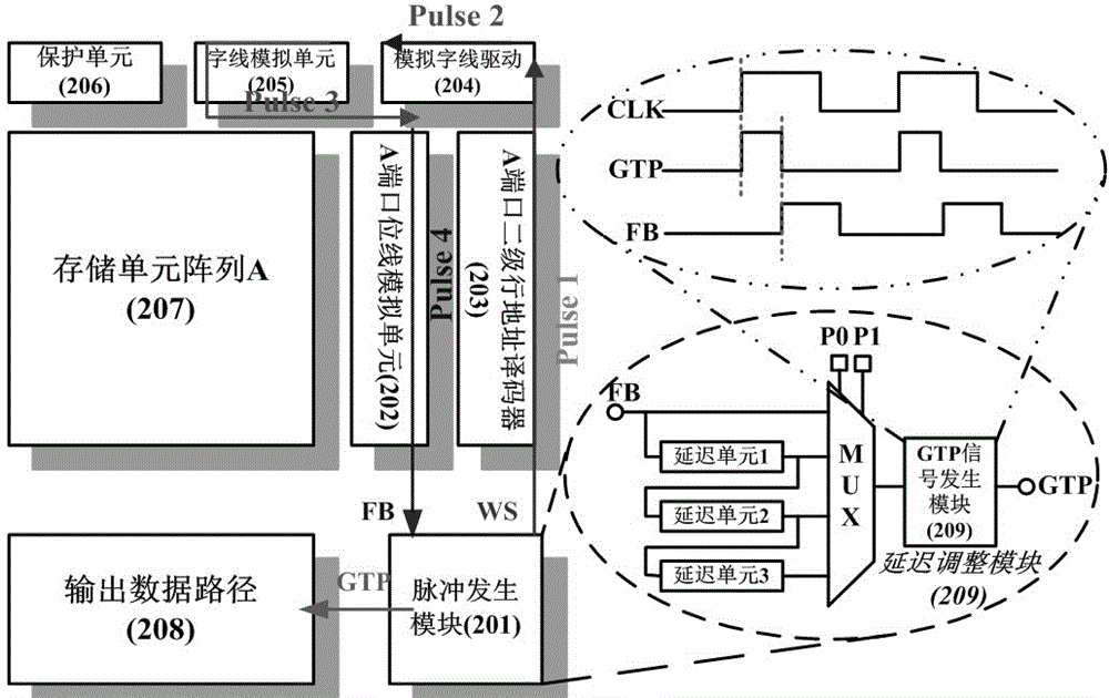
[0030] like figure 2 As shown, when the pulse generator in the overall circuit 201 After the WS work enable control signal is generated, the pulse signal Pulse1 will first pass through the word line analog drive unit 204 , the delay of the output pulse Pulse2 compared with the original pulse is that the signal passes through the analog drive unit 204 The delay; then Pulse2 input to the word line analog unit 205 , the delay of the output Pulse3 compared with Pulse2 is the delay corresponding to the signal being transmitted to the corresponding SRAM through the longest word line distance; then Pulse3 is input to the bit line analog unit 202 , the delay of the output Pulse4 compared with Pulse3 is the delay corresponding to the transmission of the signal to the corresponding SRAM through the longest bit line distance; finally the Pulse4 pulse is fed back to the pulse generation module 201 , the write / read operation is controlled by the obtained overall delay, because the dela...


PUM


Abstract

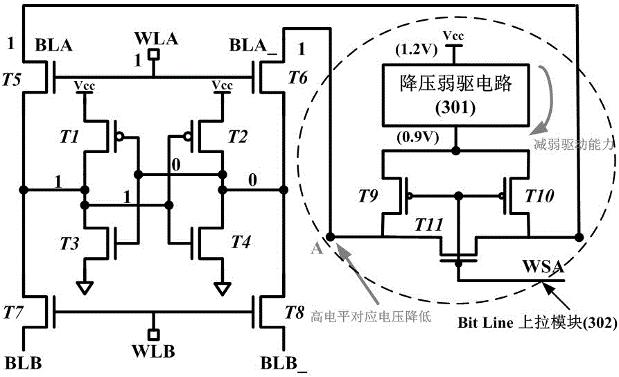
The invention belongs to the field of FPGA technology, in particular to an FPGA embedded independent dual-port BRAM IP hard core. The present invention introduces a circuit simulation delay control module into the module, dynamically simulates the transmission delay of the circuit signal under different process angles, operating temperatures and voltages, and feeds it back to the pulse generation module for control, thereby improving the asynchrony of the overall design Timing control reliability. In addition, by using high-threshold transistor SRAM to reduce static leakage power consumption, by optimizing the transmission gate size of SRAM, the drive capability of the pull-up module on the bit line is reduced to reduce the dynamic power consumption caused by the mutual pull of drive sources, thus making the BRAM IP hard Core power consumption is significantly reduced. The invention enables the programmable storage resources supported by the Block RAM to be more widely used.

Description

technical field [0001] The invention belongs to the field of FPGA technology, and in particular relates to the design and realization of an IP hard core of an independent dual-port Block RAM with high reliability and low power consumption in the FPGA. Background technique [0002] The introduction of IP hard cores such as Block RAM and DSP into FPGA, which is widely used in digital circuit design and verification, can solve the problem of performance and functional limitations of logic resources in FPGA, so that FPGA can better support large-scale applications in digital circuit design. size, high speed, and power consumption optimization requirements. [0003] Block RAM (hereinafter referred to as BRAM) is a circuit module widely used in electronic systems, mainly used to support large-scale data storage and exchange in design. Although the idea of ​​embedding BRAM into FPGA has been realized for a long time, few studies are based on optimizing the embedded hard core itsel...

Claims


Application Information

Patent Timeline
Patent Type & Authority Patents(China)
IPC IPC(8): G11C11/413
Inventor 来金梅张昕睿王键
Owner FUDAN UNIV
Learn More