OLED (organic light-emitting diode) display screen, manufacturing method for same and display device

A technology for display screens and substrates, applied in semiconductor/solid-state device manufacturing, organic semiconductor devices, electrical components, etc., can solve problems that affect production efficiency and product quality, and achieve improved production efficiency and product quality, large process error range, The effect of reducing the difficulty of debugging

Inactive Publication Date: 2014-01-08
BOE TECH GRP CO LTD
View PDF5 Cites 28 Cited by
  • Summary
  • Abstract
  • Description
  • Claims
  • Application Information

AI Technical Summary

Problems solved by technology

Therefore, when filling the filler 18 in this prior art, it is necessary to accurately control the filling amount of the fille

Method used


Image

  • OLED (organic light-emitting diode) display screen, manufacturing method for same and display device
  • OLED (organic light-emitting diode) display screen, manufacturing method for same and display device
  • OLED (organic light-emitting diode) display screen, manufacturing method for same and display device

Examples


Embodiment Construction

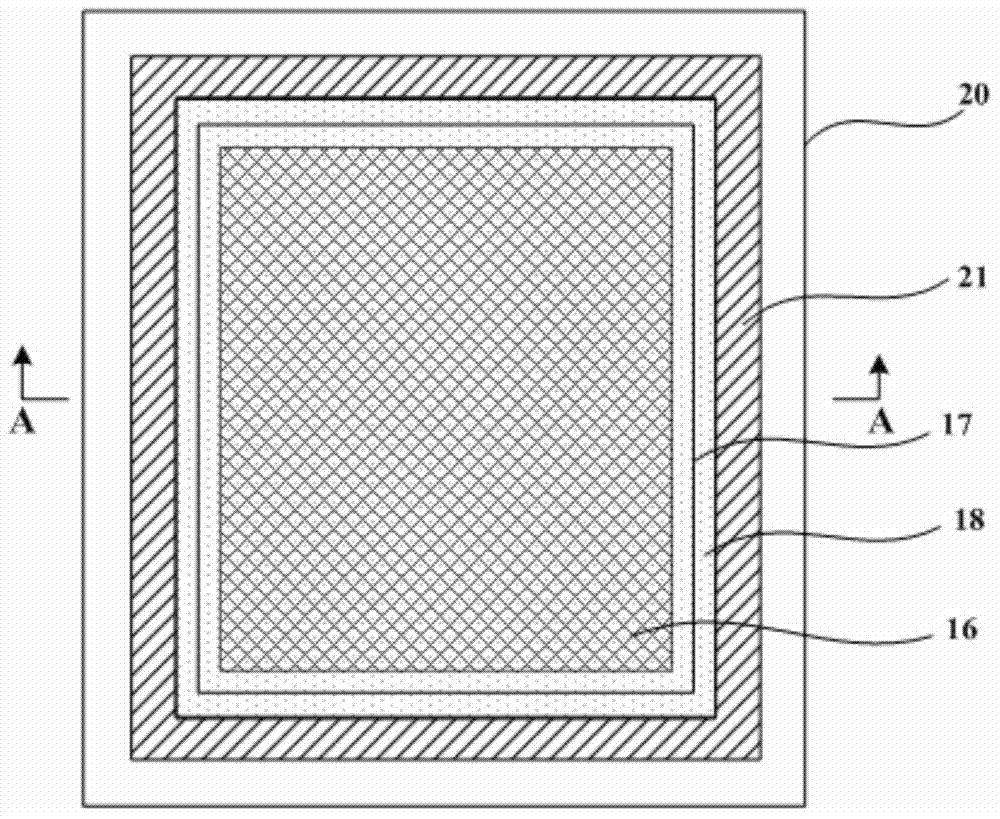
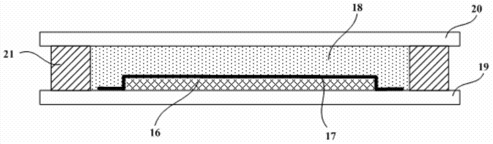
[0037] In order to reduce the difficulty of debugging the OLED display production process and improve the production efficiency and product quality of the product, embodiments of the present invention provide an OLED display, a manufacturing method of the OLED display, and a display device. In the technical solution of the OLED display screen of the present invention, two inner and outer dam glues are provided. The filler only needs to fill the inner area of ​​the first dam glue, and the excess filler can be removed from at least one opening of the first dam glue. It flows out and fills the gap area between the first dam glue and the second dam glue. With this design, the filling amount of the filler has a larger process error range compared with the prior art, and therefore, greatly reduces the OLED The difficulty of debugging the display screen production process is conducive to improving the production efficiency and product quality of the product. In order to make the objec...


PUM

PropertyMeasurementUnit
Lengthaaaaaaaaaa

Abstract

The invention discloses an OLED (organic light-emitting diode) display screen, a manufacturing method for the same and a display device, and aims to lower the debugging difficulty of an OLED display screen production process and improve the production efficiency and the quality of a product. The OLED display screen comprises a first substrate, a second substrate, first surrounding dam rubber, second surrounding dam rubber, an OLED device, a protective layer and filling rubber, wherein the first and second substrates are opposite to each other; the first surrounding dam rubber is connected between the first and second substrates, and is provided with at least one opening; the second surrounding dam rubber is connected between the first and second substrates, and is positioned outside the first surrounding dam rubber; the second surrounding dam rubber, the first substrate and the second substrate form a sealed box; the OLED device is positioned on the inner side of the first surrounding dam rubber, is positioned on the first substrate, and is covered by the protective layer; the protective layer is in sealed connection with the first substrate; the filling rubber is filled on the inner side of the first surrounding dam rubber. According to the OLED display screen, the manufacturing method for the same and the display device, the process error range of the filling volume of the filling rubber is widened, the debugging difficulty of the production process is lowered, and the production efficiency and the quality of the product are favorably improved.

Description

Technical field [0001] The present invention relates to the field of display technology, in particular to an OLED display screen, a manufacturing method of the OLED display screen and a display device. Background technique [0002] OLED (Organic Light-Emitting Diode, organic light-emitting diode, referred to as OLED) display because of its thin, light, wide viewing angle, active light emission, continuously adjustable luminous color, low cost, fast response speed, low energy consumption, and driving voltage The advantages of low temperature, wide operating temperature range, simple production process, high luminous efficiency and flexible display have been listed as the next generation display technology with great development prospects. [0003] Studies have shown that components such as water vapor and oxygen in the air have a great impact on the life of OLED devices in OLED displays. This is because: OLED devices need to inject electrons from the cathode during operation, which ...

Claims


Application Information

Patent Timeline
IPC IPC(8): H01L27/32H01L21/77
CPCH10K50/8426H10K50/846H10K50/8428H10K59/12H10K71/00H10K59/1201H10K2102/3026H10K2102/3035H01L21/77
Inventor 孙中元马凯葓
Owner BOE TECH GRP CO LTD
Why Eureka
Try Eureka