Method for photoetching of LED wafer without mask plate

A maskless and wafer-less technology, which is applied in the direction of optics, optomechanical equipment, photoplate making process of pattern surface, etc., can solve the problems of insufficient alignment accuracy of lithography machines, adhesion and bonding, and non-sticking of bonding, etc., to achieve The effect of reducing the manufacturing cost of SiO2 openings, eliminating alignment errors, and saving costs

Active Publication Date: 2014-01-15
EPILIGHT TECH
View PDF5 Cites 7 Cited by
  • Summary
  • Abstract
  • Description
  • Claims
  • Application Information

AI Technical Summary

Problems solved by technology

[0006] In view of the shortcomings of the prior art described above, the purpose of the present invention is to provide a method for photolithography LED wafers without a mask, which is used to solve the problem of SiO in the prior art. 2 Insufficient alignment accuracy of the lithography machine in the hole opening process causes SiO above the electrode 2 Can not be completely etched away, and the exfoliated SiO 2 Adhesion to the electrode causes the problem of non-sticking of subsequent wire bonding

Method used


Image

  • Method for photoetching of LED wafer without mask plate
  • Method for photoetching of LED wafer without mask plate
  • Method for photoetching of LED wafer without mask plate

Examples


Embodiment Construction

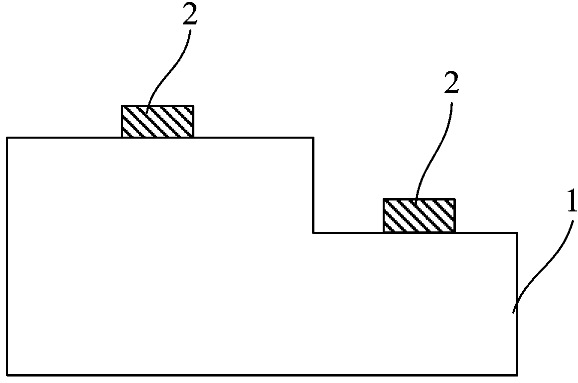
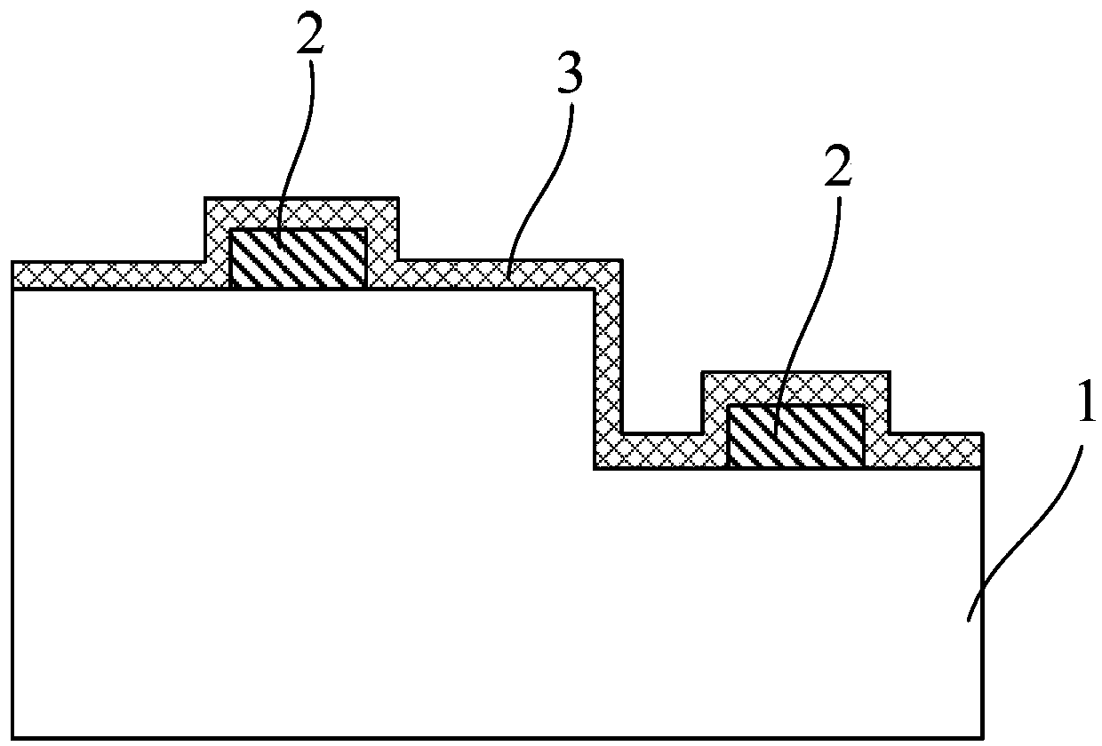
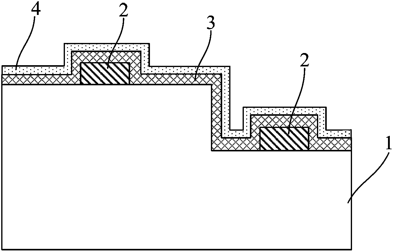
[0030] Embodiments of the present invention are described below through specific examples, and those skilled in the art can easily understand other advantages and effects of the present invention from the content disclosed in this specification. The present invention can also be implemented or applied through other different specific implementation modes, and various modifications or changes can be made to the details in this specification based on different viewpoints and applications without departing from the spirit of the present invention.

[0031] see Figure 2a to Figure 2f . It should be noted that the diagrams provided in this embodiment are only schematically illustrating the basic idea of ​​the present invention, and only the components related to the present invention are shown in the diagrams rather than the number, shape and shape of the components in actual implementation. Dimensional drawing, the type, quantity and proportion of each component can be changed a...


PUM

PropertyMeasurementUnit
thicknessaaaaaaaaaa

Abstract

The invention provides a method for photoetching of an LED wafer without a mask plate. The method makes good use of the light-proof characteristics of metal electrodes, carries out exposure on negative photoresist from the back face of the substrate of the LED wafer, achieves accurate self-aligned photoetching, and overcomes the defects that SiO2 above the electrodes cannot be etched off completely due to the fact that the alignment accuracy of a photoetching machine is insufficient in a traditional SiO2 layer trepanning technology, a SiO2 layer is made to be tightly connected with the electrodes, the SiO2 on the electrodes is completely eradicated from falling off, and therefore the problem that wires cannot be bonded in follow-up wire bonding is solved. In addition, according to the method, only a simple photoetching machine is needed, no photoetching plate is needed, the expensive cost of photoetching machine devices and photoetching plates is saved, poor products caused by alignment errors are eliminated, working efficiency is improved, and the SiO2 trepanning manufacturing cost in the manufacturing process of LED chips is reduced greatly.

Description

technical field [0001] The invention relates to a photolithography process, in particular to a method for photoetching an LED chip without a mask, and belongs to the field of semiconductor manufacturing processes. Background technique [0002] Light-emitting diodes have the advantages of small size, high efficiency and long life, and are widely used in traffic indication, outdoor full-color display and other fields. In particular, LEDs are generally considered by the industry to be the ideal choice for the fourth-generation light source due to their excellent performance. LED light sources are superior to traditional light sources such as incandescent lamps and fluorescent lamps in terms of luminous efficiency, service life, response time, and environmental protection. [0003] In the manufacture of LED chips, it is necessary to use SiO 2 protection, but want to use SiO 2 It is almost impossible to protect other positions of the electrodes just exposed, because the alignme...

Claims


Application Information

Patent Timeline
Patent Type & Authority Applications(China)
IPC IPC(8): H01L33/00G03F7/00
CPCG03F7/0035H01L33/0095H01L33/44H01L2933/0025
Inventor 袁根如郝茂盛张楠李士涛朱广敏陈诚
Owner EPILIGHT TECH
Why Eureka
Try Eureka