Light emitting diode structure and method for manufacturing thereof

A technology of light-emitting diodes and manufacturing methods, which is applied to electrical components, circuits, semiconductor devices, etc., can solve the problems of long manufacturing process time, poor productivity, high labor and manufacturing process costs

Inactive Publication Date: 2014-01-15
CHI MEI LIGHTING TECH +1
View PDF3 Cites 0 Cited by
  • Summary
  • Abstract
  • Description
  • Claims
  • Application Information

AI Technical Summary

Problems solved by technology

[0006] Although the light extraction efficiency of the light-emitting diode structure 100a is better than that of the light-emitting diode structure 100, the manufacturing process of the distributed Bragg reflector 124 is complicated and difficult. It will also cause a decrease in the yield of the manufacturing process

Method used


Image

  • Light emitting diode structure and method for manufacturing thereof
  • Light emitting diode structure and method for manufacturing thereof
  • Light emitting diode structure and method for manufacturing thereof

Examples


Embodiment Construction

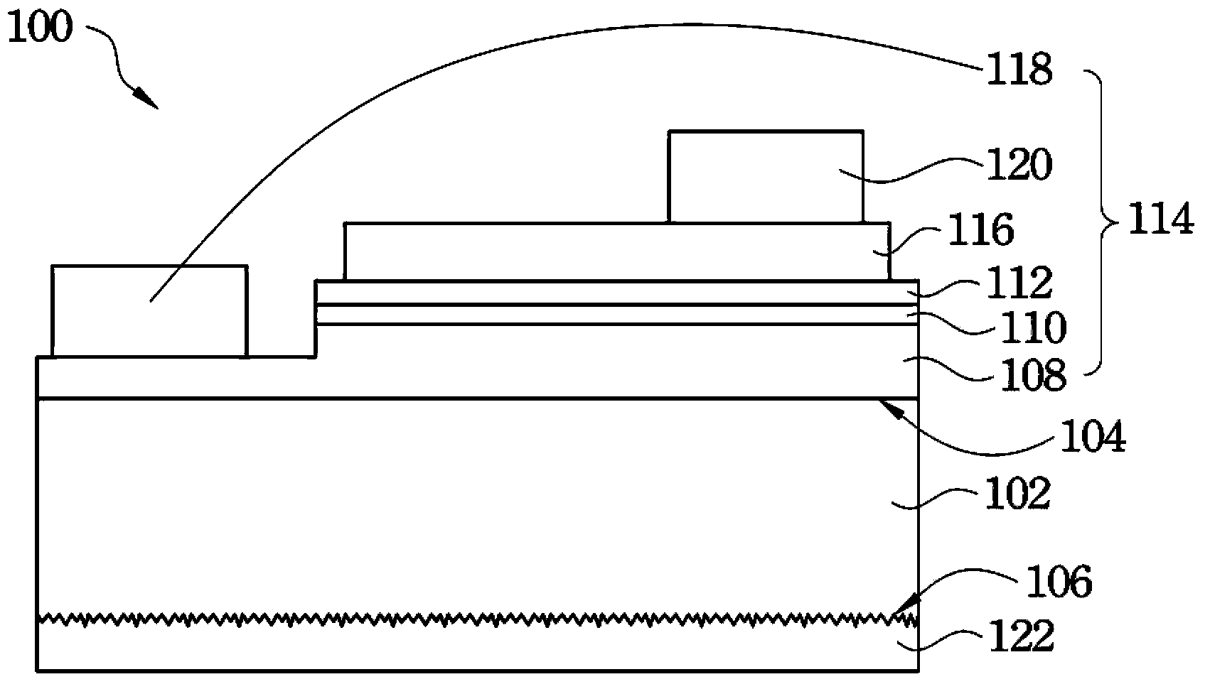
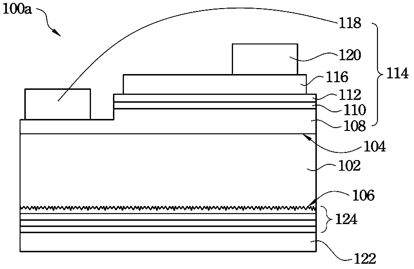
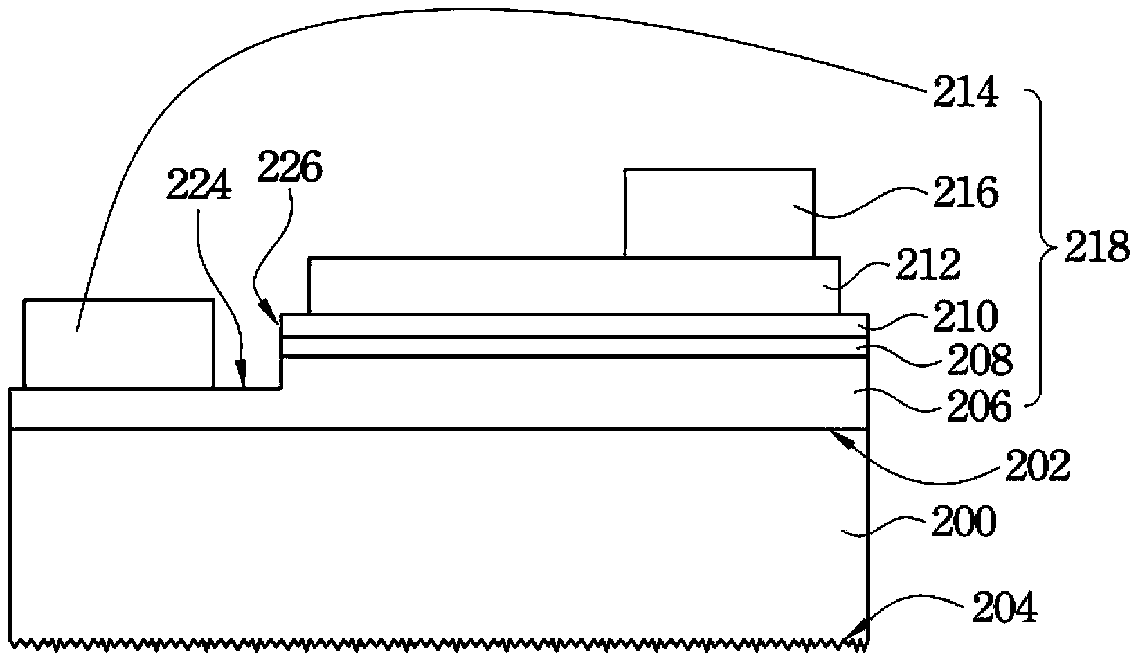
[0045] Please refer to Figure 3A to Figure 3C , which is a cross-sectional view illustrating a manufacturing process of a light emitting diode structure according to an embodiment of the present invention. In this embodiment, the light emitting diode structure 222 mainly includes a transparent substrate 200, a light emitting structure 218 and a metal reflector 220, such as Figure 3C shown. The LED structure 222 only includes a single metal reflector 220, but does not have the distributed Bragg reflectors of conventional LED structures.

[0046] Such as Figure 3A As shown, when fabricating the LED structure 222, the transparent substrate 200 is provided first. The transparent substrate 200 includes surfaces 202 and 204 , wherein the surfaces 202 and 204 are respectively located on opposite sides of the transparent substrate 200 . The transparent substrate 200 can be, for example, a sapphire substrate.

[0047]Next, a light emitting structure 218 is formed on the surface...


PUM

PropertyMeasurementUnit
mean roughnessaaaaaaaaaa
particle diameteraaaaaaaaaa

Abstract

The invention discloses a light emitting diode structure and a method for manufacturing thereof. The method for manufacturing the light emitting diode structure comprises the following steps: providing a transparent substrate, wherein the transparent substrate comprising a first surface and an opposite second surface; forming a light emitting structure on the first surface; performing thinning processing on the second surface of the transparent substrate so as to reduce thickness of the transparent substrate; performing planarization processing on the second surface after the thinning processing; and forming a metal mirror covering the second surface which is processed by the planarization processing.

Description

technical field [0001] The present invention relates to a light-emitting element, and in particular to a light-emitting diode (LED) structure and a manufacturing method thereof. Background technique [0002] Please refer to figure 1 , which is a cross-sectional view illustrating a conventional LED structure. The conventional LED structure 100 includes a transparent substrate 102 , a light emitting structure 114 and a metal mirror 122 . Opposite sides of the transparent substrate 102 have surfaces 104 and 106 respectively. The light emitting structure 114 is disposed on the surface 104 of the transparent substrate 102 . The light emitting structure 114 includes an n-type semiconductor layer 108 , an active layer 110 , a p-type semiconductor layer 112 , a transparent conductive layer 116 , an n-type electrode pad 118 and a p-type electrode pad 120 sequentially stacked on the surface 104 of the transparent substrate 102 . Wherein, the n-type electrode pad 118 is disposed on...

Claims


Application Information

Patent Timeline
Patent Type & Authority Applications(China)
IPC IPC(8): H01L33/10H01L33/00
CPCH01L33/20H01L33/46H01L2933/0016H01L2933/0025H01L2933/0058
Inventor 江宗儒
Owner CHI MEI LIGHTING TECH
Why Eureka
Try Eureka