Manufacturing method for improving accuracy of PCB (printed circuit board) back drilling hole

A technology of PCB board and production method, which is applied in the directions of printed circuit manufacturing, electrical components, printed circuits, etc., can solve problems such as the deviation of the bottom hole position of back drilling and through holes, and achieve the effect of improving accuracy and ensuring flatness.

Active Publication Date: 2014-01-22
广东依顿电子科技股份有限公司
View PDF5 Cites 36 Cited by
  • Summary
  • Abstract
  • Description
  • Claims
  • Application Information

AI Technical Summary

Problems solved by technology

[0005] 3. The PCB board will expand and shrink by 0-2mil during the process from drilling the through hole to the back drilling process. If the back drilling board directly corresponds to the original through hole drilling tape coefficient, it is easy to cause back drilling and through holes due to expansion and contraction. There is a positional deviation of 0-2mil i

Method used


Image

  • Manufacturing method for improving accuracy of PCB (printed circuit board) back drilling hole
  • Manufacturing method for improving accuracy of PCB (printed circuit board) back drilling hole

Examples


Embodiment Construction

[0030] The present invention will be further described in detail below in conjunction with specific embodiments.

[0031] A manufacturing method for improving the accuracy of drilling holes on the back of a PCB, comprising the following steps:

[0032] 1) Cutting - cutting a whole copper clad laminate, cleaning the surface and baking and dehumidifying the whole board;

[0033] 2) Transfer of inner layer circuit pattern and circuit inspection - paste a layer of photosensitive material on the copper foil of the above-mentioned circuit board, and then carry out alignment exposure through black film, form a circuit pattern after development, and drill pipe position holes on the edge of the board, And use automatic optical detection equipment to detect whether there is a bad circuit opening or short circuit on the circuit board surface;

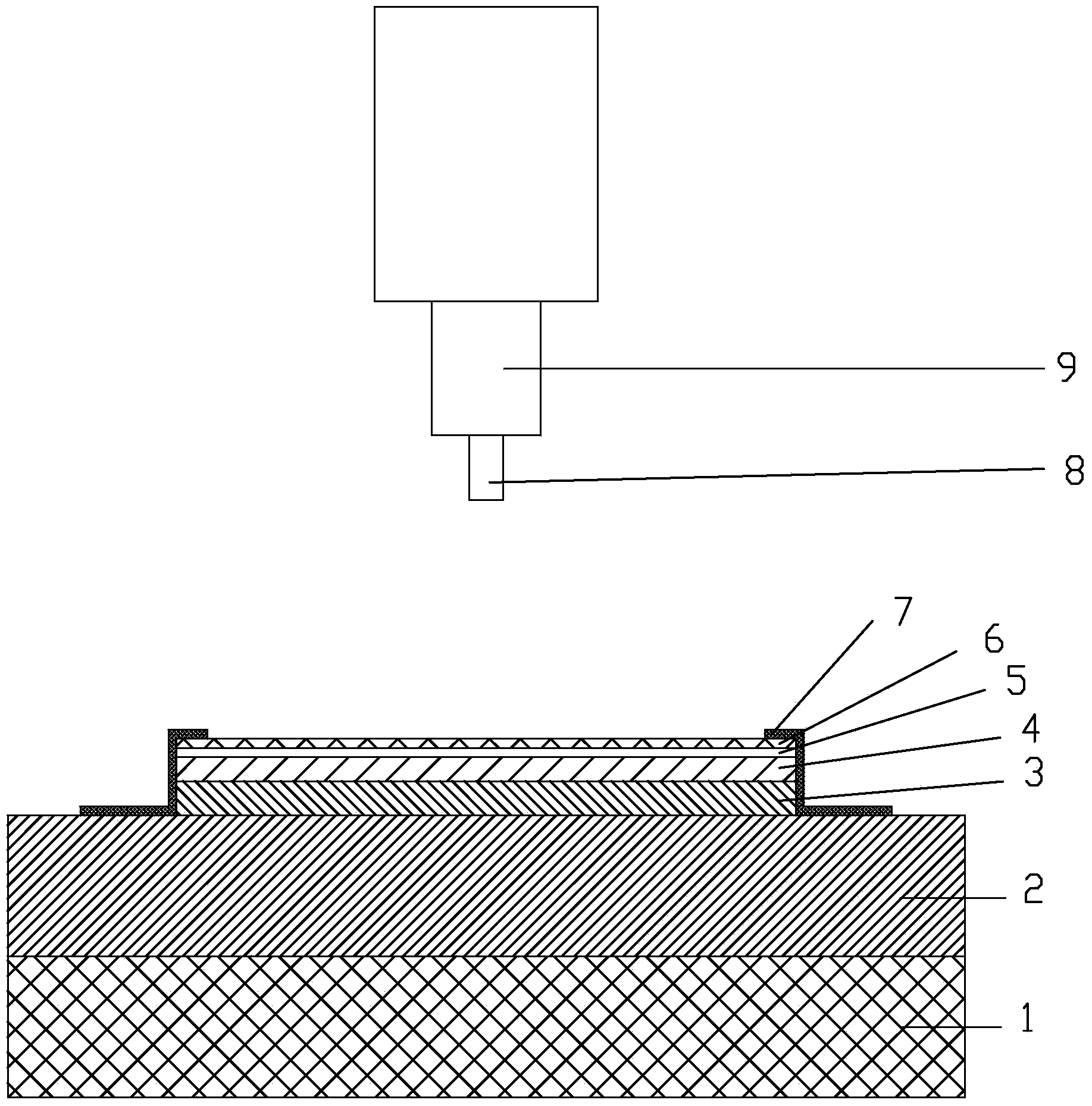
[0034] 3) Pressing plate - stack and press the above circuit substrate and resin prepreg according to the design to obtain a laminated circuit b...


PUM

PropertyMeasurementUnit
Thicknessaaaaaaaaaa

Abstract

The invention discloses a manufacturing method for improving accuracy of a PCB back drilling hole. The manufacturing method comprises the steps as follows: A), a circuit board substrate is subjected to front procedure processing, through-hole drilling, copper deposition, board electroplating, outer circuit pattern transferring, pattern electroplating and the like; B), back drilling is performed on a PCB 4, and whether the depth of the back drilling hole is qualified is detected; and C), a well drilled back drilling hole is subjected to alkaline etching and photosensitive welding resistance, and finally a finished product is manufactured. The technical scheme is characterized in that drill file coefficients used in a through-hole drilling procedure are correspondingly corrected according to expansion and contraction data obtained in a technological process from the through-hole drilling procedure to the drilling procedure of the PCB 4 during back drilling, and the drill file data is maintained to be consistent with actual expansion and contraction; a drilling-in surface in the through-hole drilling procedure is consistent with that during the back drilling; and a phenolic aldehyde base plate 6 is additionally paved on the top surface of the PCB 4. With the adoption of the manufacturing method, the depth accuracy and the position accuracy of a back drilling hole of a conventional PCB 4 can be effectively improved, so that the completeness of signal transmission of the PCB 4 is guaranteed.

Description

【Technical field】 [0001] The invention relates to the technical field of PCB manufacturing, in particular to a process flow and method design for manufacturing back-drilled holes on a PCB. 【Background technique】 [0002] PCB board back-drilling technology refers to mechanically drilling off the unnecessary transmission conductive layer on the sunken copper hole for conduction, so that the reserved part can stabilize the signal. It is mainly used to ensure the stability of PCB serial data transmission and achieve high-speed The role of signal transmission. Back-drilling technology is more and more widely used on high-frequency circuit boards. However, the existing back-drilling technology has the following problems: [0003] 1. The existing back drilling depth accuracy control method is to use a back drilling rig with a depth control function, position the back drilling PCB board pin on the drilling rig table, and then cover a thin aluminum sheet on the surface of the PCB b...

Claims


Application Information

Patent Timeline
IPC IPC(8): H05K3/00
Inventor 莫介云
Owner 广东依顿电子科技股份有限公司
Why Eureka
Try Eureka