
Ultra-narrow frame liquid crystal display and chip-on-film (COF) packaging structure of drive circuit thereof

A liquid crystal display, packaging structure technology, applied in static indicators, instruments, nonlinear optics, etc., can solve the problems of shrinking cross-sectional area, rising resistance, rising resistance per unit length, etc., to avoid panel color unevenness, improve quality, the effect of avoiding pressure drop

Active Publication Date: 2014-02-05
TCL CHINA STAR OPTOELECTRONICS TECH CO LTD
View PDF6 Cites 18 Cited by
  • Summary
  • Abstract
  • Description
  • Claims
  • Application Information

AI Technical Summary

Problems solved by technology

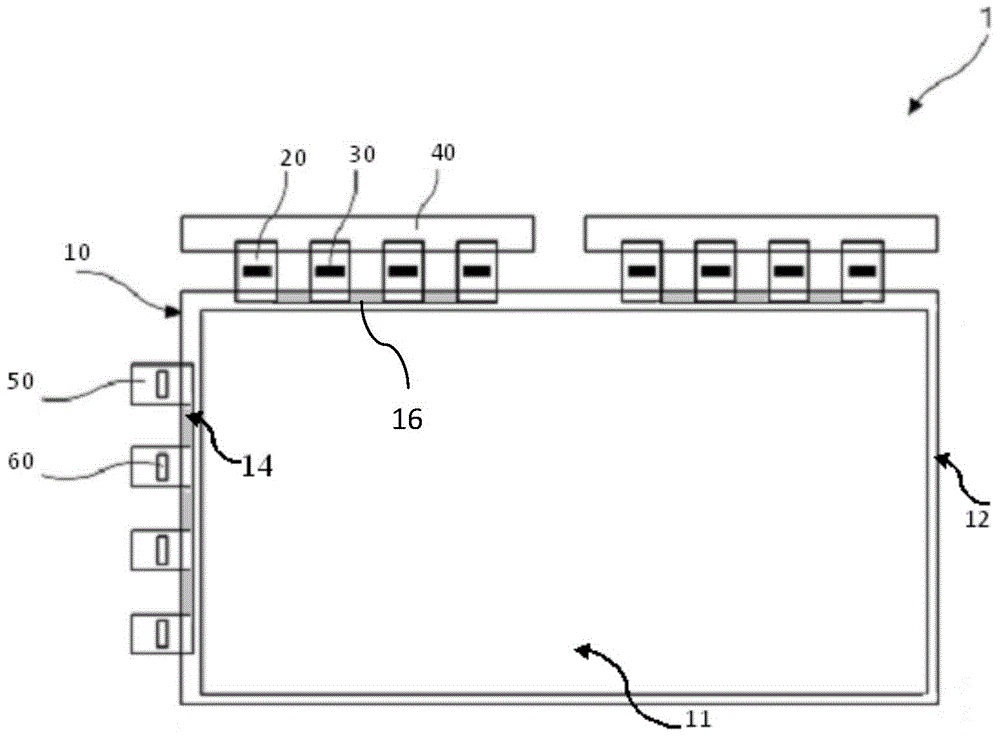
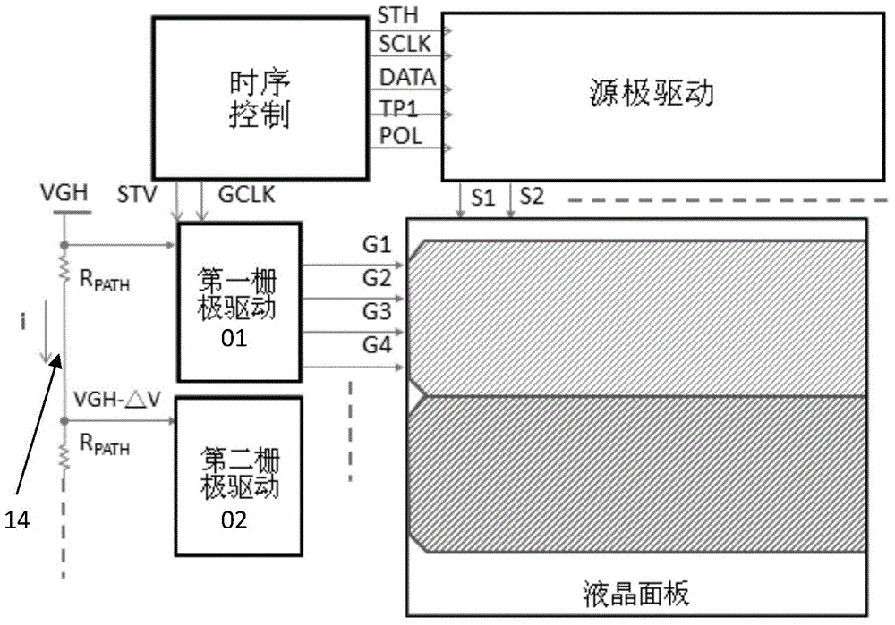
[0009] Due to the trend of narrowing the frame, that is, minimizing the frame area 12, the width of the wiring 14 will be narrowed along with the narrowing of the edge width of the glass substrate, and its cross-sectional area will be reduced, resulting in a resistance per unit length. If the value increases, if the panel size becomes larger, the trace will become longer and the resistance value will also increase

Method used


Image

  • Ultra-narrow frame liquid crystal display and chip-on-film (COF) packaging structure of drive circuit thereof
  • Ultra-narrow frame liquid crystal display and chip-on-film (COF) packaging structure of drive circuit thereof
  • Ultra-narrow frame liquid crystal display and chip-on-film (COF) packaging structure of drive circuit thereof

Examples


Embodiment Construction

[0030] In order to make the object, technical solution and advantages of the present invention clearer, the present invention will be further described in detail below in conjunction with the accompanying drawings.

[0031] In order to make the above objects, features and advantages of the present invention more comprehensible, preferred embodiments of the present invention will be described in detail below together with the accompanying drawings. In order to make the above objects, features and advantages of the present invention more comprehensible, preferred embodiments of the present invention will be described in detail below together with the accompanying drawings. Furthermore, the directional terms mentioned in the present invention, such as "up", "down", "front", "rear", "left", "right", "inside", "outside", "side", etc., It is only for orientation with reference to the attached drawings. Therefore, the directional terms used are used to illustrate and understand the ...


PUM


Abstract

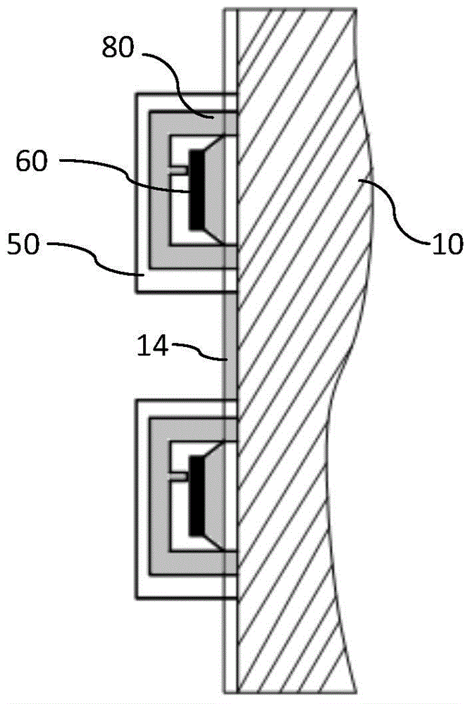
The invention discloses an ultra-narrow frame liquid crystal display and a chip-on-film (COF) packaging structure of a drive circuit thereof. The packaging structure comprises a whole flexible circuit board, wherein one side of the whole flexible circuit board is jointed with a frame region of a glass substrate of the liquid crystal display, and the whole flexible circuit board serves as a COF type flexibly-packaged carrier band. Multiple drive chips are respectively jointed with the whole flexible circuit board in the scanning direction in sequence, and signal circuits among adjacent drive chips are arranged on the whole flexible circuit board. In the COF packaging structure, the whole flexible circuit board is utilized to move the signal circuits required by drive integrated circuits (IC) to a COF from the glass substrate, so that pressure drop caused by wiring resistance value increase of the drive IC during large-size ultra-narrow frame design can be avoided, a phenomenon that the large-size ultra-narrow frame enables input voltage transferred to the drive IC to produce pressure drop and accordingly panel color is uneven is avoided, and the product quality is improved.

Description

technical field [0001] The invention relates to the field of liquid crystal display, in particular to a COF packaging structure of an ultra-narrow frame liquid crystal display and a driving circuit thereof. Background technique [0002] Nowadays, in order to meet the needs of various high-density packaging, the semiconductor packaging industry has gradually developed various types of packaging designs. The design concepts of various packaging structures are mostly to make high-density packaging products thinner and more suitable for In increasingly thinner and shorter electronic products, such as narrow bezel LCDs. [0003] In liquid crystal modules using light-emitting diode backlight modules, narrow bezel design is a trend. At present, the thickness of mature product modules can be less than 5 cm (mm), and there is a design requirement for ultra-narrow bezels. , especially in the design of large-size, high-resolution modules. In order to implement narrow bezel design, an...

Claims


Application Information

Patent Timeline
Patent Type & Authority Applications(China)
IPC IPC(8): G02F1/133
CPCG02F1/13452G02F1/133G02F1/13306
Inventor 张峻恺吴智豪
Owner TCL CHINA STAR OPTOELECTRONICS TECH CO LTD
Learn More