Method for extracting graphic features of layout of chip and CMP simulation method

A graphic feature and layout technology, applied in special data processing applications, instruments, calculations, etc., can solve problems such as inaccurate simulation results, achieve accurate prediction, and improve accuracy

Active Publication Date: 2014-02-05
INST OF MICROELECTRONICS CHINESE ACAD OF SCI
View PDF3 Cites 27 Cited by
  • Summary
  • Abstract
  • Description
  • Claims
  • Application Information

AI Technical Summary

Problems solved by technology

[0006] However, the simulation results obtained by using the above-mentioned method of extracting layout graphic features for CMP process simulation are often inaccurate

Method used


Image

  • Method for extracting graphic features of layout of chip and CMP simulation method
  • Method for extracting graphic features of layout of chip and CMP simulation method
  • Method for extracting graphic features of layout of chip and CMP simulation method

Examples


Embodiment 1

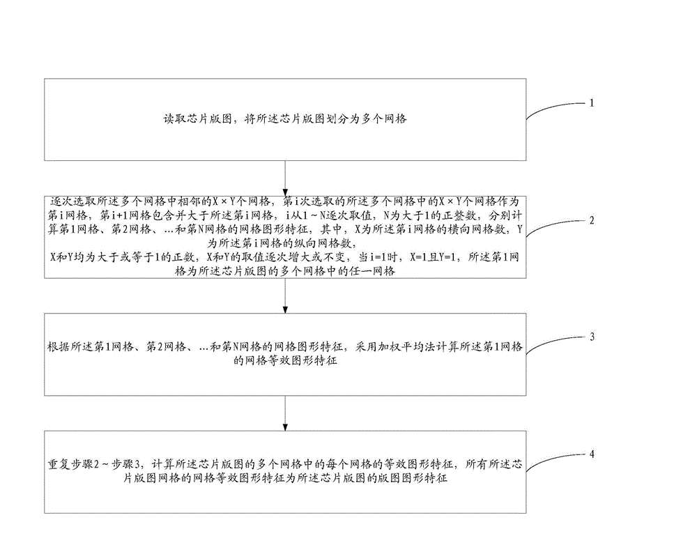
[0054] This embodiment provides a method for extracting layout graphic features of chip layout, such as figure 1 As shown, the method includes the following steps:

[0055] Step 1: read the chip layout, and divide the chip layout into multiple grids;

[0056] Considering that the current chip layout is usually a hierarchical structure, a preprocessing step of flattening the chip layout is required before layout division.

[0057] In order to reduce the amount of calculation, the plurality of divided grids are preferably squares with the same size. However, in actual application, the layout can also be divided into grids of other shapes as required, and the sizes of the divided grids can be different.

[0058] Due to the different ups and downs in different areas of the chip layout, the size of the divided grid needs to be selected. Generally, the principle of selecting the grid size is: not less than the planarization length of the layout; the so-called planarization length ...

Embodiment 2

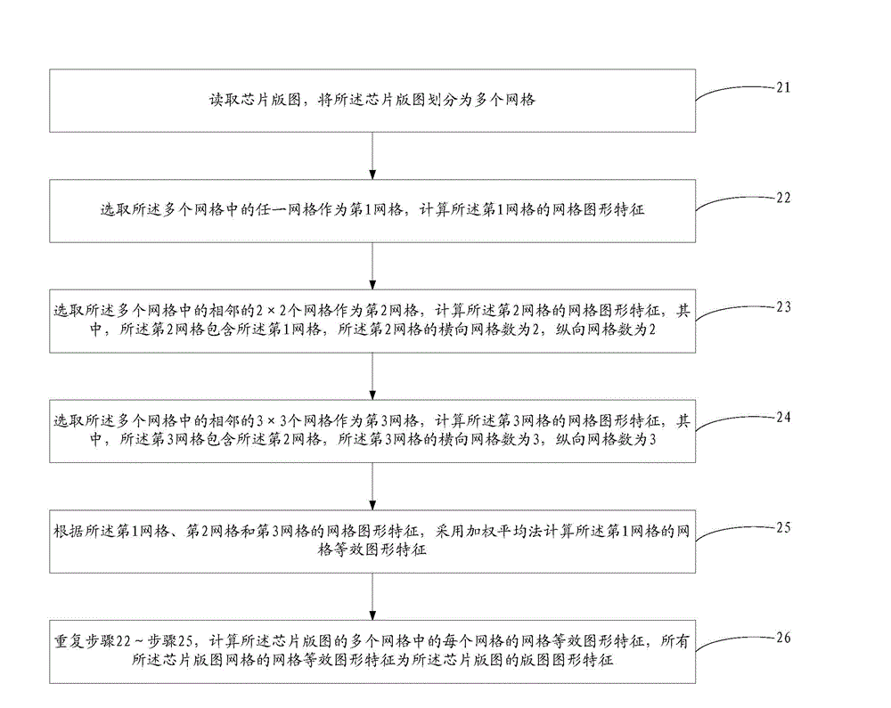
[0090] Based on Embodiment 1, this embodiment specifically introduces the method provided in Embodiment 1 by taking N=3 as an example. N=3 means that multiple grids of the chip layout are selected three times. Such as figure 2 As shown, the method includes the following steps:

[0091] Step 21: read the chip layout, and divide the chip layout into multiple grids;

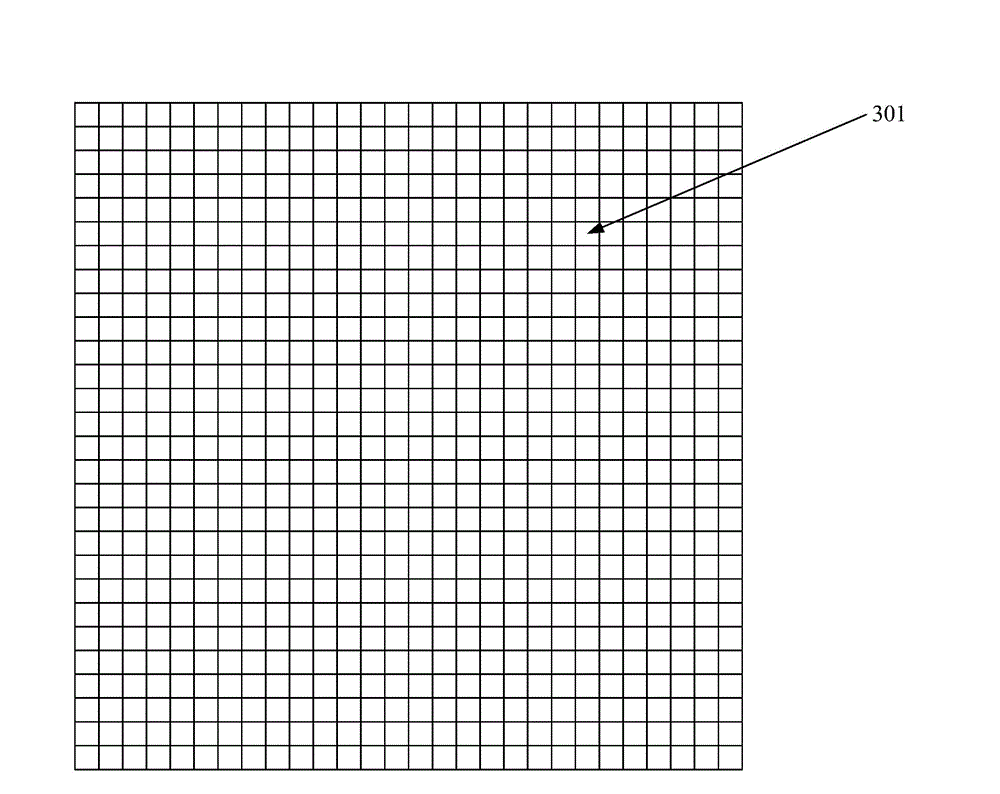
[0092] Such as image 3 As shown, the chip layout is divided into a plurality of square grids 301 with the same shape and size, the size of the grid 301 is less than or equal to the planarization length of the chip layout, and the size of the grid 301 is D 1 .

[0093] Step 22: selecting any one of the plurality of grids as the first grid, and calculating the grid graphic features of the first grid;

[0094] Such as Figure 4 As shown, select any grid as the first grid 401, and the size of the first grid 401 is D 2 , the first grid 401 contains a plurality of graphic areas, and these graphic areas are defined...

Embodiment 3

[0111] Based on embodiment one and embodiment two, this embodiment provides a kind of CMP emulation method, and this method comprises the following steps:

[0112] Using the method described in Embodiment 1 and Embodiment 2 to extract the layout graphic features of the chip layout;

[0113] A CMP model is selected, and the layout graphic features of the chip layout are used as parameters of the CMP model to perform CMP process simulation.

[0114] The CMP simulation method provided in this embodiment can consider the proximity effect of different graphics in the layout to a greater extent, and consider various characteristic parameters of the layout graphics in a more comprehensive manner. The simulation accuracy is high, and the calculation amount is small, which is convenient for implementation; Assisting the foundry to realize the process prediction can save the cost of process tape-out and testing, and enable the foundry to produce chips that meet the design ideas of the c...


PUM


Abstract

The invention provides a method for extracting graphic features of the layout of a chip and a CMP (chemical mechanical polishing) simulation method. In the process of extracting the graphic features of the layout, an incremental partition method is adopted, firstly, the layout of the chip is partitioned into a plurality of grids, then any one grid is selected, the graphic feature of the selected grid is calculated, based on the grid, the size of the grid is gradually increased, the graphic feature of the grid after each increase in size is calculated, a method of weighted mean is adopted to calculate to obtain an equivalent grid graphic feature of the selected grid, then the same method is adopted to calculate to obtain the equivalent grid graphic feature of each of the rest grids of the layout of the chip, and all equivalent grid graphic features are used as the graphic features of the layout. According to the method, the incremental partition method is adopted as a correlative mechanism about proximity effects of all partitioned grids of the layout of the chip, the graphic proximity effects of different grids in the CMP process are taken into full consideration, the accurate prediction about the surface topography of the layout of the chip is realized, and the accuracy in simulation in the CMP process is improved.

Description

technical field [0001] The invention relates to the technical field of CMP process simulation, and more specifically, relates to a method for extracting layout graphic features of a chip layout and a CMP simulation method. Background technique [0002] CMP (Chemical Mechanical Polishing) is the mainstream planarization process of current semiconductor processing technology. It achieves the purpose of planarizing the wafer surface by combining chemical abrasives and mechanical polishing. The mechanism is roughly that there is a large amount of polishing liquid containing quartz sand abrasive particles on the polishing pad, and the surface material of the wafer, especially the surface material with raised parts, chemically reacts with the polishing liquid to form a surface layer that is relatively easy to remove. The surface layer is mechanically abraded off under the pressure of the abrasive grains and relative motion with the polishing pad, thereby flattening the wafer surfa...

Claims


Application Information

Patent Timeline
Patent Type & Authority Applications(China)
IPC IPC(8): G06F17/50
Inventor 刘宏伟陈岚孙艳张贺方晶晶
Owner INST OF MICROELECTRONICS CHINESE ACAD OF SCI
Why Eureka
Try Eureka