
Method for manufacturing wafer full-color LED display array

A display array, wafer-level technology, used in semiconductor/solid-state device manufacturing, instruments, electrical components, etc., can solve the limitation of miniaturization of LEDRGB full-color packaging unit size, the pixel size of full-color LED screen cannot be reduced, and the impact on the final LED screen pixel resolution and other issues, to achieve the effect of simplifying the preparation process

Active Publication Date: 2014-02-12
INST OF SEMICONDUCTORS - CHINESE ACAD OF SCI
View PDF4 Cites 24 Cited by
  • Summary
  • Abstract
  • Description
  • Claims
  • Application Information

AI Technical Summary

Problems solved by technology

[0005] In the process of realizing the present invention, the applicant found that the size miniaturization of the LED RGB full-color packaging unit is limited due to the limitations of the soldering process, the alignment accuracy of the die-bonding machine, and the aperture of the conductive through hole.
It directly affects the pixel resolution of the final LED screen, so the pixel size of the full-color LED screen cannot be reduced, and the minimum size can only be about 1mm

Method used


Image

  • Method for manufacturing wafer full-color LED display array
  • Method for manufacturing wafer full-color LED display array
  • Method for manufacturing wafer full-color LED display array

Examples


Embodiment Construction

[0027] In order to make the object, technical solution and advantages of the present invention clearer, the present invention will be described in further detail below in conjunction with specific embodiments and with reference to the accompanying drawings. It should be noted that, in the drawings or descriptions of the specification, similar or identical parts all use the same figure numbers. Implementations not shown or described in the accompanying drawings are forms known to those of ordinary skill in the art. Additionally, while illustrations of parameters including particular values ​​may be provided herein, it should be understood that the parameters need not be exactly equal to the corresponding values, but rather may approximate the corresponding values ​​within acceptable error margins or design constraints. The directional terms mentioned in the embodiments, such as "upper", "lower", "front", "rear", "left", "right", etc., are only referring to the directions of the...


PUM


Abstract

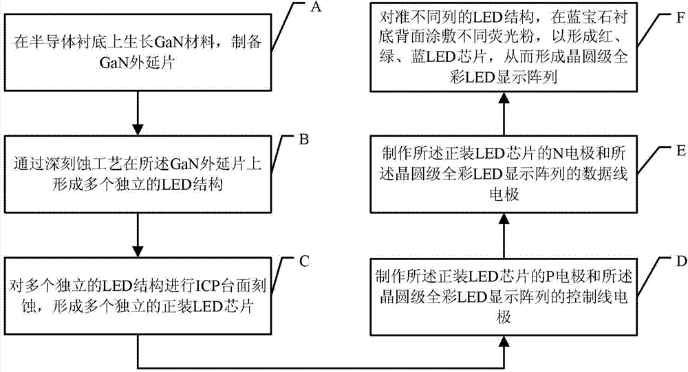
The invention provides a method for manufacturing a wafer full-color LED display array. The method for manufacturing the wafer full-color LED display array includes the following steps that firstly, a GaN material grows on a substrate and a GaN epitaxial wafer is manufactured; secondly, multiple isolated LED structures are formed on the GaN epitaxial wafer through a deep etching technology; sixthly, the LED structures of different rows are directed and different fluorescent powder coats the back of the sapphire substrate to form a red, green and blue LED chip and thus, the wafer full-color LED display array is formed. According to the method for manufacturing the wafer full-color LED display array, the fluorescent powder coats the LED sapphire substrate row by row so as to directly achieve full-color display on the LED sapphire wafer and thus, the pixel size of the wafer LED display array is less than 500 microns.

Description

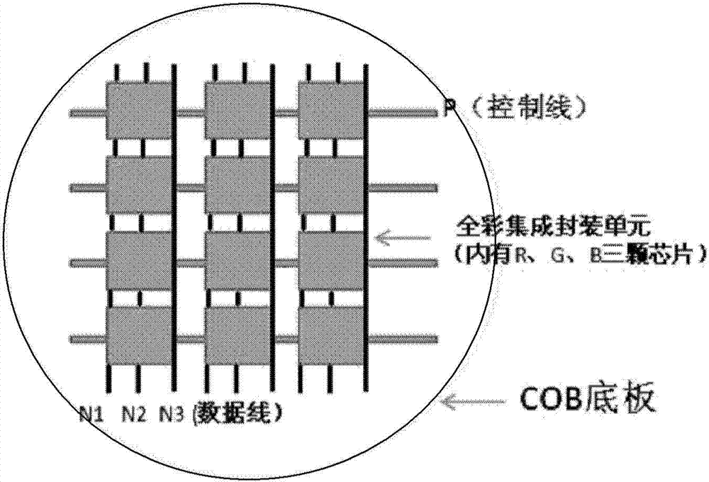
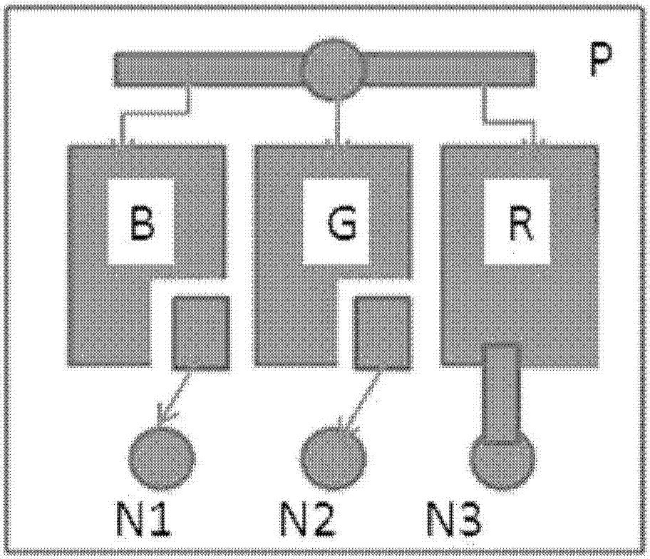
technical field [0001] The invention relates to the technical field of optoelectronic devices, in particular to a method for preparing a wafer-level full-color LED display array. Background technique [0002] LED display is a new type of information display media that developed rapidly in the world in the late 1980s. It uses LED light-emitting diodes to form a dot matrix module or pixel unit to form a large-area display screen. In addition to significant energy-saving effects, it also has reliability. High performance, long service life, strong environmental adaptability, high price-performance ratio, low cost of use, and large-area display, etc., have rapidly grown into mainstream products in the field of flat-panel display in just over ten years, and have gained recognition in the field of information display. widely used. [0003] In the past, LEDs were generally used for indoor and outdoor super-large screen displays, and now they are widely used in sports facilities, p...

Claims


Application Information

Patent Timeline
IPC IPC(8): H01L33/48H01L33/50H01L33/62G09F9/33
CPCH01L21/0242H01L21/02458H01L21/0254H01L21/0262H01L21/3065H01L27/15H01L33/0066H01L33/50H01L2933/0016H01L2933/0041
Inventor 李璟杨华薛斌王国宏王军喜李晋闽
Owner INST OF SEMICONDUCTORS - CHINESE ACAD OF SCI
Learn More