Solid State Imaging Apparatus Method for Fabricating the Same and Camera Using the Same

a technology of solid-state imaging and camera, which is applied in the field of solid-state imaging apparatus, can solve the problems of difficult to reduce the size of the pixel, and achieve the effect of increasing the area of the light-receiving area and reducing the pixel siz

Active Publication Date: 2008-05-08
GK BRIDGE 1
View PDF14 Cites 14 Cited by
  • Summary
  • Abstract
  • Description
  • Claims
  • Application Information

AI Technical Summary

Benefits of technology

[0026]A solid state imaging apparatus of the present invention, a method for fabricating the same and a camera using the same achieve reduction in the pixel size and increase in the area of a light-receiving area while securing the electrical isolation property of an isolation region. In addition, a solid state imaging apparatus allowing only small numbers of random noises and white defects, a fabrication method for the same and a camera can be achieved.

Problems solved by technology

This makes it difficult to reduce the size of the pixel.

Method used


Image

  • Solid State Imaging Apparatus Method for Fabricating the Same and Camera Using the Same
  • Solid State Imaging Apparatus Method for Fabricating the Same and Camera Using the Same
  • Solid State Imaging Apparatus Method for Fabricating the Same and Camera Using the Same

Examples


embodiment 1

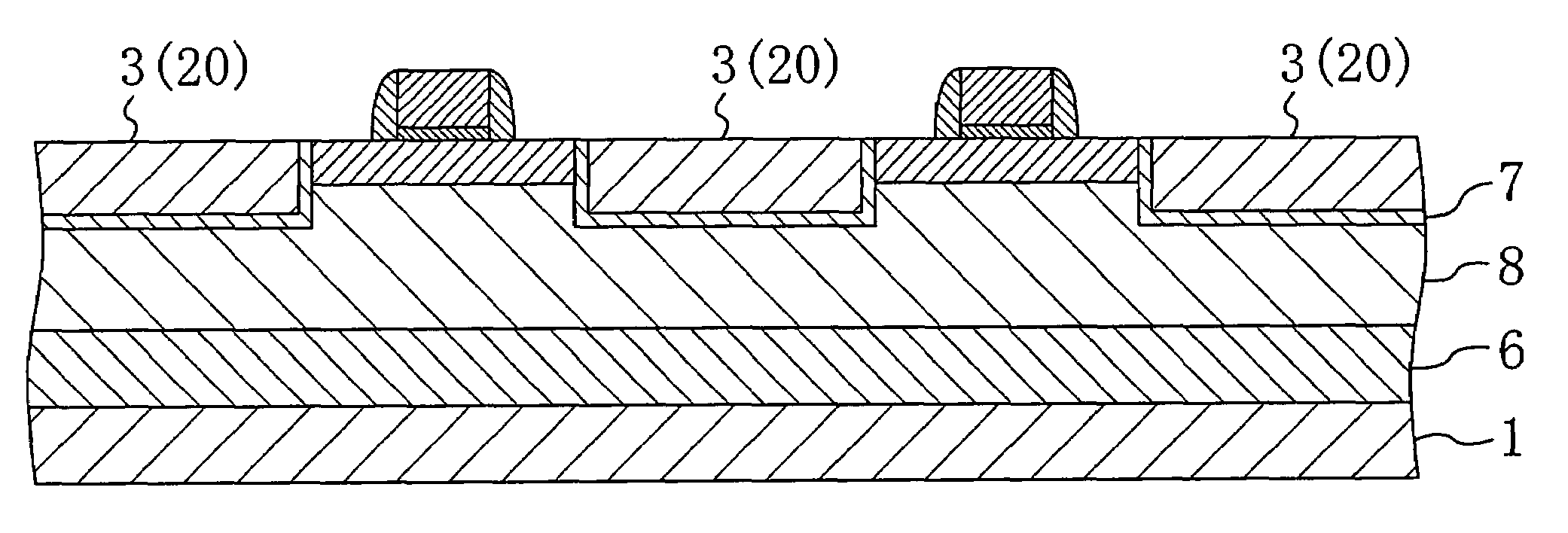
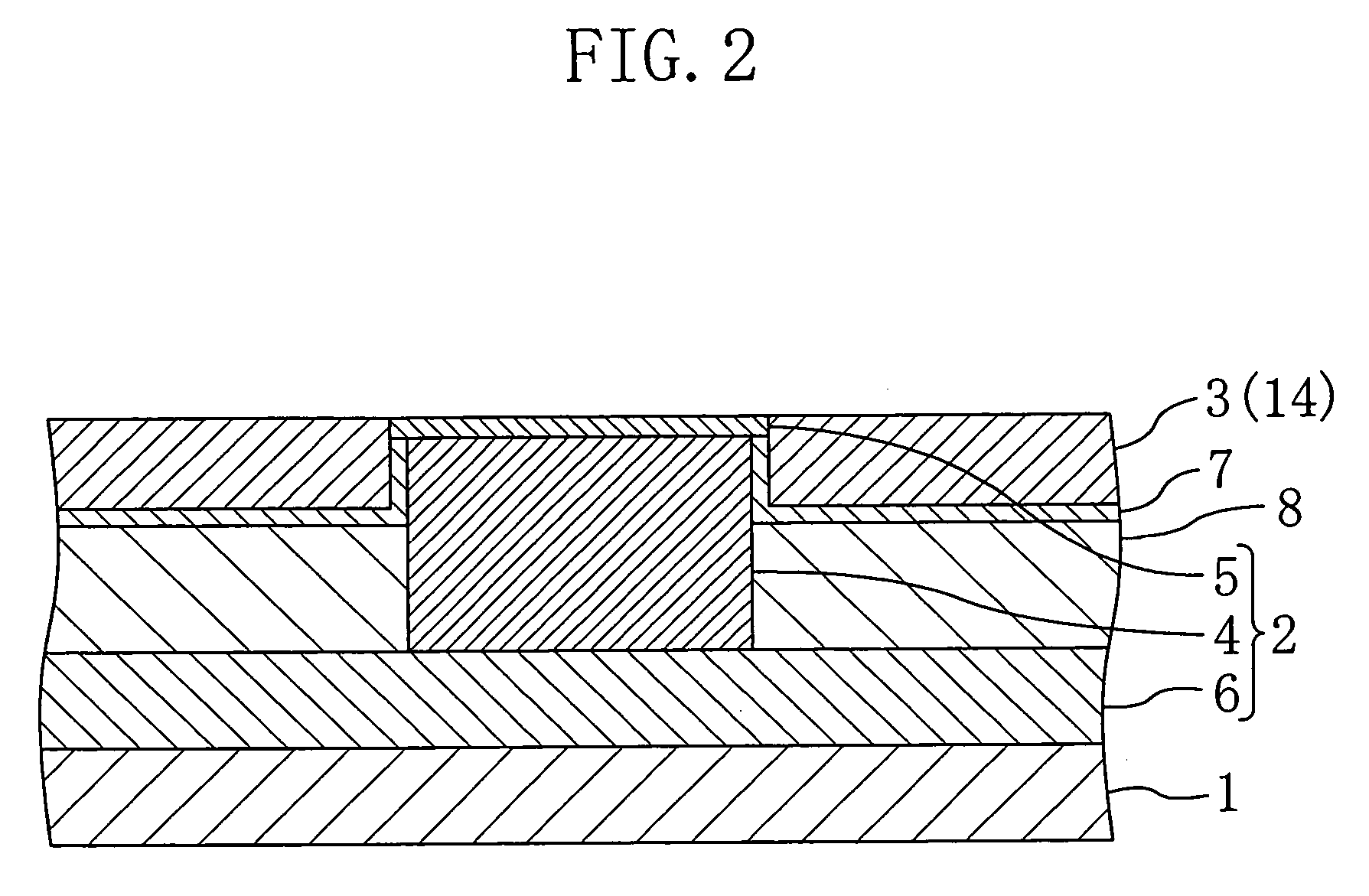
[0098]A solid state imaging apparatus according to a first embodiment of the present invention and a fabrication method for the same will be described hereinafter with reference to the drawings.

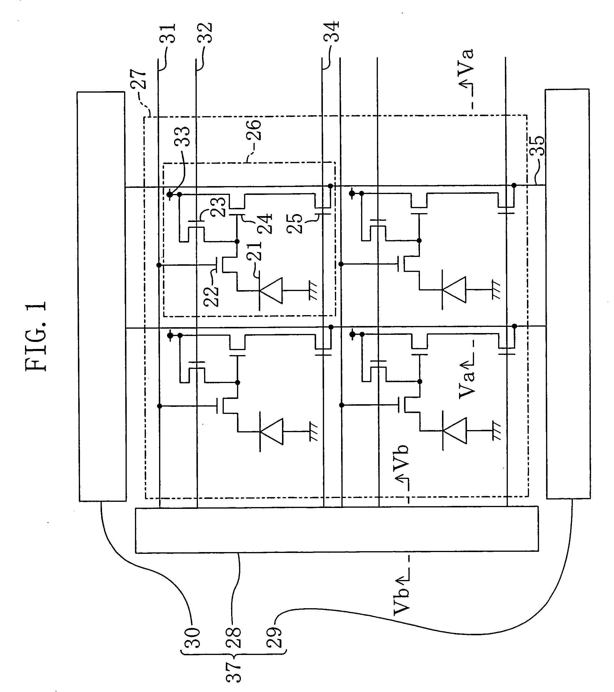
[0099]FIG. 1 illustrates a circuit diagram of a CMOS solid state imaging apparatus of this embodiment. As illustrated in FIG. 1, an imaging area 27 in which a plurality of pixels 26 are arranged in matrix, a vertical shift register 28 and a horizontal shift register 29 each for selecting a pixel, and a timing generator circuit 30 for supplying a necessary pulse to the vertical shift register 28 and the horizontal shift register 29 are formed on one substrate.

[0100]Each of the pixels 26 arranged in the imaging area 27 is composed of a photodiode 21 serving as a photoelectric conversion section and associated semiconductor devices. A transfer transistor 22 is connected at its source to an output part of the photoelectric conversion section 21. Connected to the drain of a transfer transistor 22 ...

embodiment 2

Modification of Embodiment 2

[0153]A solid state imaging apparatus according to a modification of a second embodiment of the present invention will be described hereinafter with reference to the drawings.

[0154]The solid state imaging apparatus of this modification is characterized in that an isolation region 3 illustrated in FIG. 7 is formed of a P-type porous silicon.

[0155]FIGS. 10(a) through 10(d) are cross-sectional views illustrating process steps in a fabrication method for the solid state imaging apparatus of this modification step by step.

[0156]First, as illustrated in FIG. 10(a), a resist (not shown) is formed to have an opening in its predetermined region, and ions are implanted into a substrate 1 of semiconductor using the resist as a mask, thereby forming a P-type silicon section 16 containing a P-type impurity in predetermined part of the substrate 1 of semiconductor.

[0157]Next, as illustrated in FIG. 10(b), an electrode for anodization is formed on part of the P-type sil...

embodiment 3

[0164]A solid state imaging apparatus according to a third embodiment of the present invention and a fabrication method for the same will be described hereinafter with reference to the drawings.

[0165]FIG. 11 is a cross-sectional view illustrating a photodiode section of the solid state imaging apparatus of this embodiment. In FIG. 11, the same reference numerals are given to the same components as in FIG. 2, and a description thereof is not given. In this embodiment, an isolation region 3 is formed of a silicon film 41 and a porous silicon film 42 to reduce the stress in heat treatment. As illustrated in FIG. 11, a U-shaped porous silicon film 42 is embedded in the silicon film 41.

[0166]FIGS. 12(a) through 12(e) are cross-sectional views illustrating process steps in the fabrication method for the solid state imaging apparatus step by step.

[0167]First, as illustrated in FIG. 12(a), a pad insulating film 10 made of a silicon oxide film is formed on a substrate 1 of silicon to have a ...


PUM


Abstract

A solid state imaging apparatus includes a plurality of photoelectric conversion sections formed in an imaging area of a silicon substrate, and an embedded layer embedded in an isolation trench formed in at least one part of the silicon substrate located around the photoelectric conversion sections. The embedded layer is made of an isolation material having a thermal expansion coefficient larger than silicon oxide and equal to or smaller than silicon.

Description

TECHNICAL FIELD[0001]The present invention relates to a solid state imaging apparatus in which an imaging area including a plurality of pixels is formed at part of a substrate, a method for fabricating the same, and a camera.BACKGROUND ART[0002]A complementary-metal-oxide-semiconductor (CMOS) solid state imaging apparatuses represents an image sensor in which a signal accumulated in a photodiode forming part of each of pixels is read out by an amplifier circuit including a MOS transistor. Such a CMOS solid state imaging apparatus can operate at low voltages, consume less power, and be integrated in one chip together with a peripheral circuit.[0003]In view of the above, attention has been paid to CMOS solid state imaging apparatuses as image input devices used for compact cameras for personal computers and portable devices, such as cell phones. In recent years, an increase in the number of pixels have been demanded for CMOS solid state imaging apparatuses, and therefore the cell size...

Claims


Application Information

Patent Timeline
Patent Type & Authority Applications(United States)
IPC IPC(8): H01L29/76H01L29/94H01L31/00H01L21/8238H01L27/146H04N5/335H04N5/367H04N5/369H04N5/374
CPCH01L27/14603H01L27/14689H01L27/14643H01L27/1463
Inventor MORI, MITSUYOSHIUEDA, DAISUKE
Owner GK BRIDGE 1
Why Eureka
Try Eureka