Monocrystalline silicon substrate TFT device

A monocrystalline silicon and substrate technology, applied in semiconductor devices, semiconductor/solid-state device manufacturing, transistors, etc., can solve problems such as performance gaps and achieve the effect of reducing pixel size

Inactive Publication Date: 2015-06-03
SHANGHAI JIAO TONG UNIV
View PDF7 Cites 14 Cited by
  • Summary
  • Abstract
  • Description
  • Claims
  • Application Information

AI Technical Summary

Problems solved by technology

The active layer in this technology uses polysilicon islands. Although the process has been improved, there is still a big gap between performance and monocrystalline silicon islands.

Method used


Image

  • Monocrystalline silicon substrate TFT device
  • Monocrystalline silicon substrate TFT device
  • Monocrystalline silicon substrate TFT device

Examples


Embodiment 1

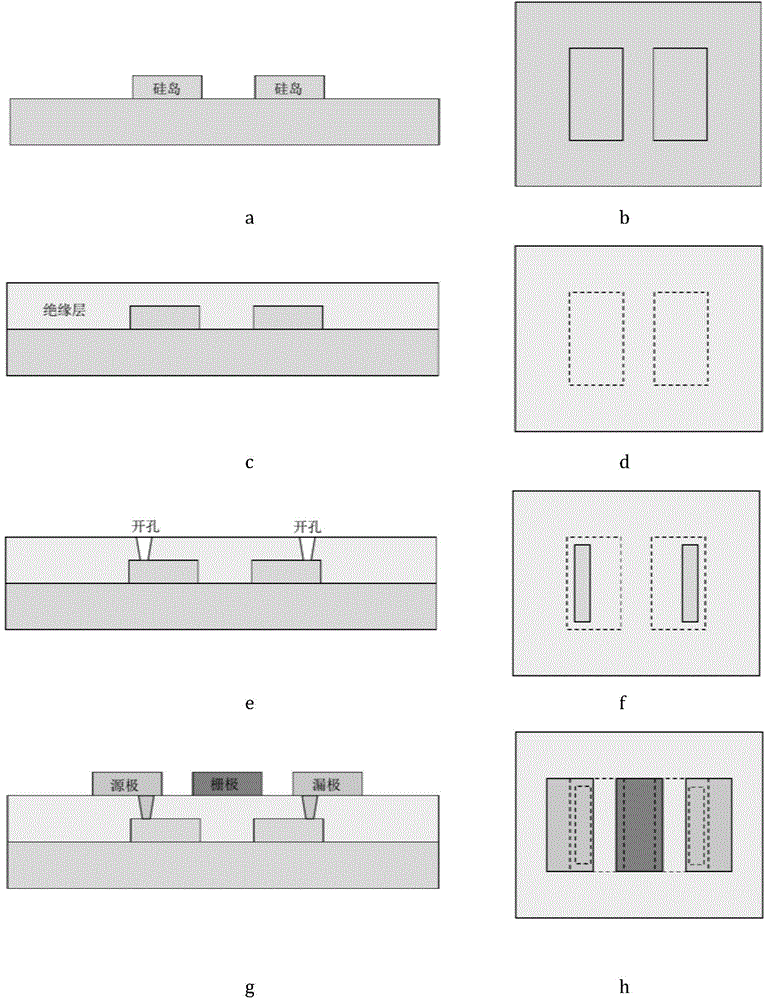
[0022] Such as figure 1 As shown in a to h, this embodiment includes the following steps:

[0023] 1. If figure 1 a and figure 1 As shown in b, the silicon island is etched on the single crystal silicon substrate. The etching method can be directly etched by laser beam, or ion beam etching can be used after covering the protective layer on the single crystal silicon substrate, or other etching methods can be used method. The size of the silicon island to be etched depends on the design requirements of the device.

[0024] 2. If figure 1 c and figure 1 As shown in d, the etched silicon island is covered with a layer of insulating material, which can be done by evaporation or magnetron sputtering, or by sol-gel method. The insulating material can be inorganic substances such as metal oxides and metal salts, or organic materials. The insulating material used should have good adhesion to the single crystal silicon substrate and be compatible with the subsequent process. sex...

Embodiment 2

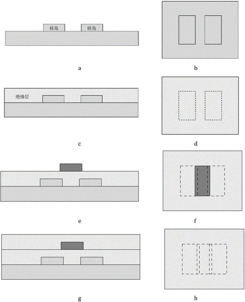
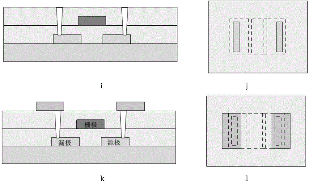
[0029] Such as figure 2 Shown in a~l, this embodiment includes the following steps:

[0030] 1. If figure 2 a and figure 2 As shown in b, the silicon island is etched on the single crystal silicon substrate. The etching method can be directly etched by laser beam, or ion beam etching can be used after covering the protective layer on the single crystal silicon substrate, or other etching methods can be used method. The size of the silicon island to be etched depends on the design requirements of the device.

[0031] 2. If figure 2 c and figure 2 As shown in d, the etched silicon island is covered with a layer of insulating material, which can be done by evaporation or magnetron sputtering, or by sol-gel method. The insulating material can be inorganic substances such as metal oxides and metal salts, or organic materials. The insulating material used should have good adhesion to the single crystal silicon substrate and be compatible with the subsequent process. sex....


PUM


Abstract

The invention discloses a monocrystalline silicon substrate TFT (thin-film transistor) device belonging to the field of semiconductor device preparation. Silicon islands serving as source and drain foundations are etched on the surface of monocrystalline silicon; the surface of each silicon island is covered by at least one layer of insulating material and is perforated; then a gate, a source and a drain are respectively manufactured on one layer or different layers of the insulating materials; finally the source and the drain are connected with the corresponding silicon islands to form the TFT device. The TFT device disclosed by the invention takes the monocrystalline silicon as a substrate; the silicon islands are etched on the monocrystalline silicon substrate and are used as the source and the drain of the TFT device; therefore the performance of the TFT device can be greatly improved.

Description

technical field [0001] The present invention relates to a technology in the field of semiconductor device preparation, in particular to a single crystal silicon substrate TFT (Thin-Film Transistor, thin film transistor) device. Background technique [0002] There are mainly three kinds of active layer materials of existing TFT devices: organic materials (such as pentacene), metal oxides (such as IGZO), and silicon materials (such as amorphous silicon and polysilicon). The performance of these three materials is limited, and the carrier mobility of organic materials generally does not exceed 1cm 2 / Vs, the carrier mobility of amorphous IGZO is about 3-15cm 2 / Vs, polycrystalline IGZO can reach 50cm 2 / Vs or so, the carrier mobility of amorphous silicon is at 1cm 2 / Vs or so, polysilicon can reach 100 ~ 200cm 2 / Vs, in contrast, the carrier mobility of single crystal silicon is about 1500cm 2 / Vs or so, compared with the other three materials, the performance is improved ...

Claims


Application Information

Patent Timeline
Patent Type & Authority Applications(China)
IPC IPC(8): H01L29/786H01L21/336
CPCH01L29/786H01L21/28H01L29/66742
Inventor 王东平谢应涛方汉铿
Owner SHANGHAI JIAO TONG UNIV
Why Eureka
Try Eureka