Ultra-wide dynamic range image sensor based on pixel charge compensation technology

An image sensor and wide dynamic range technology, applied in image communication, color TV components, TV system components, etc., can solve problems such as complex circuit structure, lower pixel filling ratio, complex external reading and storage circuits, etc.

Active Publication Date: 2012-10-24
JILIN UNIV
View PDF3 Cites 14 Cited by
  • Summary
  • Abstract
  • Description
  • Claims
  • Application Information

AI Technical Summary

Problems solved by technology

It is mainly achieved by increasing the parasitic capacitance around the DP or other gate capacitance structures, but this method will reduce the filling ratio of the pixel and reduce the response characteristics under weak light
(2) Multiple sampling technology, that is, to sample the same scene through multiple exposures, this method requires more complex external reading and storage circuits, and is not suitable for high-speed photography scenes
(3) Multi-detector pixels, that is, two photodiodes are integrated in one pixel unit, one for weak light conditions and one for strong light conditions, but its circuit structure is complex, and the problem of potential well capacity is not fundamentally solved , limited ability to increase DR
[0008] In addition, there are other more complex ways to improve the dynamic range, but so far there is no ideal method

Method used


Image

  • Ultra-wide dynamic range image sensor based on pixel charge compensation technology
  • Ultra-wide dynamic range image sensor based on pixel charge compensation technology
  • Ultra-wide dynamic range image sensor based on pixel charge compensation technology

Examples


Embodiment 1

[0038] The image sensor of the present invention is fully compatible with the standard CMOS process. An image sensor array composed of a 320×240 area array will be described in detail below based on the 0.18 μm standard CMOS process, with reference to the drawings and embodiments.

[0039] Device system design

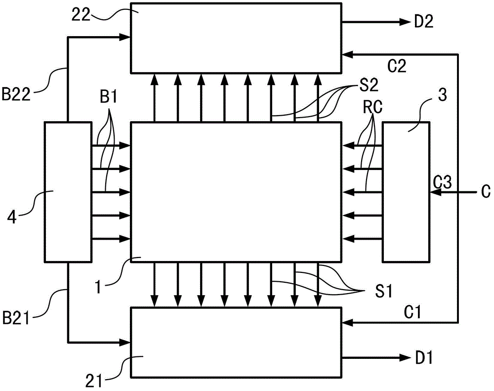
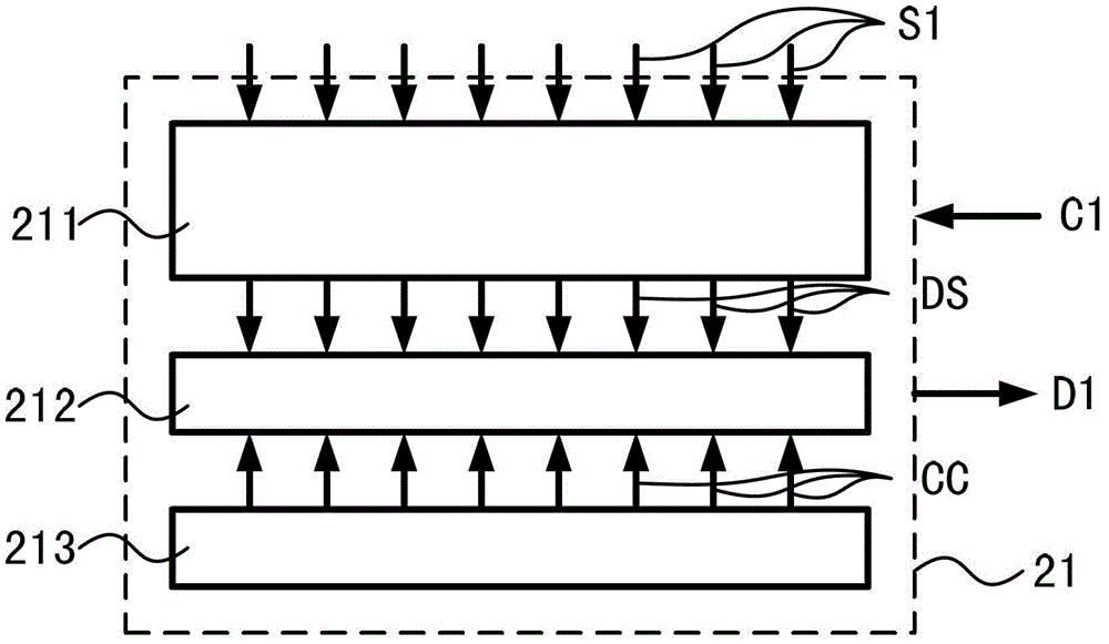
[0040] In this specific embodiment, the image sensor is designed under the standard 0.18 μm CMOS process. The system architecture adopts figure 1 structure shown. The pixel array in the designed module 1 is arranged into 240 rows and 320 columns, such as Figure 7 shown. Each pixel unit adopts such as Figure 4 In the 3T structure shown, the pixel output S1 of each column is connected to the signal bus Signal Bus. And set the current source load I on the bus Signal Bus1~SignalBus 320 of each column B1 ~ I B320 . As the light intensity changes continuously, the pixel array generates a continuously changing voltage signal. This signal is generated by the row dec...


PUM


Abstract

The invention belongs to the technical field of semiconductor image sensing, and relates to an ultra-wide dynamic range image sensor based on a pixel charge compensation technology. The ultra-wide dynamic range image sensor based on the pixel charge compensation technology is composed of a photoelectric conversion module 1, an upper read-out processing module 21 and a lower read-out processing module 22 for controlling and reading out data of the photoelectric conversion module 1, a column decoding module 3 and an offset signal module 4. A pixel element is integrated with an element for charge compensation near a main photodiode, so pixel output saturation is avoided by compensating charge to an integrating capacitor of the main photodiode under a highlight condition. An apparatus forms a linear response as to the light intensity under a weak light condition, and the linear response is automatically converted into the linear response to a light intensity logarithm under a strong light condition, so as to obtain an extremely wide dynamic range; the amplitude of the output voltage of a pixel circuit is large; a column amplifier circuit does not need to be integrated; an analogue-digital convertor can be directly input; the design flow of the device is simplified; the chip area is saved; and the photoreceptive dynamic range is extremely wide, and the theoretical value can reach up to 200dB.

Description

technical field [0001] The invention belongs to the technical field of semiconductor image sensing, in particular to an ultra-wide dynamic range image sensor based on pixel charge compensation technology. Background technique [0002] With the development of modern information technology, image acquisition and processing technology has also been improved accordingly. As the basic equipment of image processing, image sensor is being widely used in various fields. [0003] Electronic image sensors based on semiconductor technology and processes mainly include charge-coupled devices (CCD) and CMOS image sensors (CIS). Among them, CIS adopts standard CMOS technology, is easy to integrate with circuits, and has a series of advantages such as low power consumption and low cost. In recent years, it has been more and more widely used, especially in the fields of professional photography and other fields. [0004] Dynamic range (DR) is an important index of CIS, which is used to cal...

Claims


Application Information

Patent Timeline
Patent Type & Authority Applications(China)
IPC IPC(8): H04N5/355H04N5/374H01L27/146
Inventor 常玉春李兆涵周泉宋静怡杜国同余昭杰李靖李冰
Owner JILIN UNIV
Why Eureka
Try Eureka