Thin Film Transistor, Method For Making The Same, Device Having The Same

A technology of thin-film transistors and manufacturing methods, which is applied in the direction of transistors, semiconductor/solid-state device manufacturing, semiconductor devices, etc., and can solve the problems of carrier inflow, low mobility, and inability to obtain IGZO single-film field-effect mobility.

Active Publication Date: 2012-04-04
SAMSUNG DISPLAY CO LTD
View PDF5 Cites 44 Cited by
  • Summary
  • Abstract
  • Description
  • Claims
  • Application Information

AI Technical Summary

Problems solved by technology

[0018] In Patent Document 2, since amorphous silicon whose mobility is about an order of magnitude lower than that of an oxide semiconductor is used in the carrier traveling layer as a quantum well portion, sufficient mobility cannot be obtained.
In addition, there is a problem that a good joint interface cannot be obtained by joining an IGZO film which is an oxide semiconductor to a dissimilar semiconductor material such as a-Si which is a non-oxide.
[0019] In Patent Document 3, as a method of increasing the on / off ratio without impairing the carrier concentration of the IGZO film used as the active layer, a method of inserting a resistance layer between the electrode layer and the active layer is proposed, but the method based on electron affinity is not considered. Therefore, there is a problem that the field-effect mobility exceeding the mobility of the conventional IGZO single film cannot be obtained because there is not enough carrier flow from the resistive layer to the active layer.

Method used


Image

  • Thin Film Transistor, Method For Making The Same, Device Having The Same
  • Thin Film Transistor, Method For Making The Same, Device Having The Same
  • Thin Film Transistor, Method For Making The Same, Device Having The Same

Examples


Embodiment 1

[0212] The mobilities of Examples 1, 2, and 3, and Comparative Examples 1 and 2 were compared for fabrication of bottom-gate thin-film transistors. Table 4 is a table showing Ga / (In+Ga) of each transistor, oxygen partial pressure / argon partial pressure and mobility during film formation.

[0213] [Table 4]

[0214]

[0215]

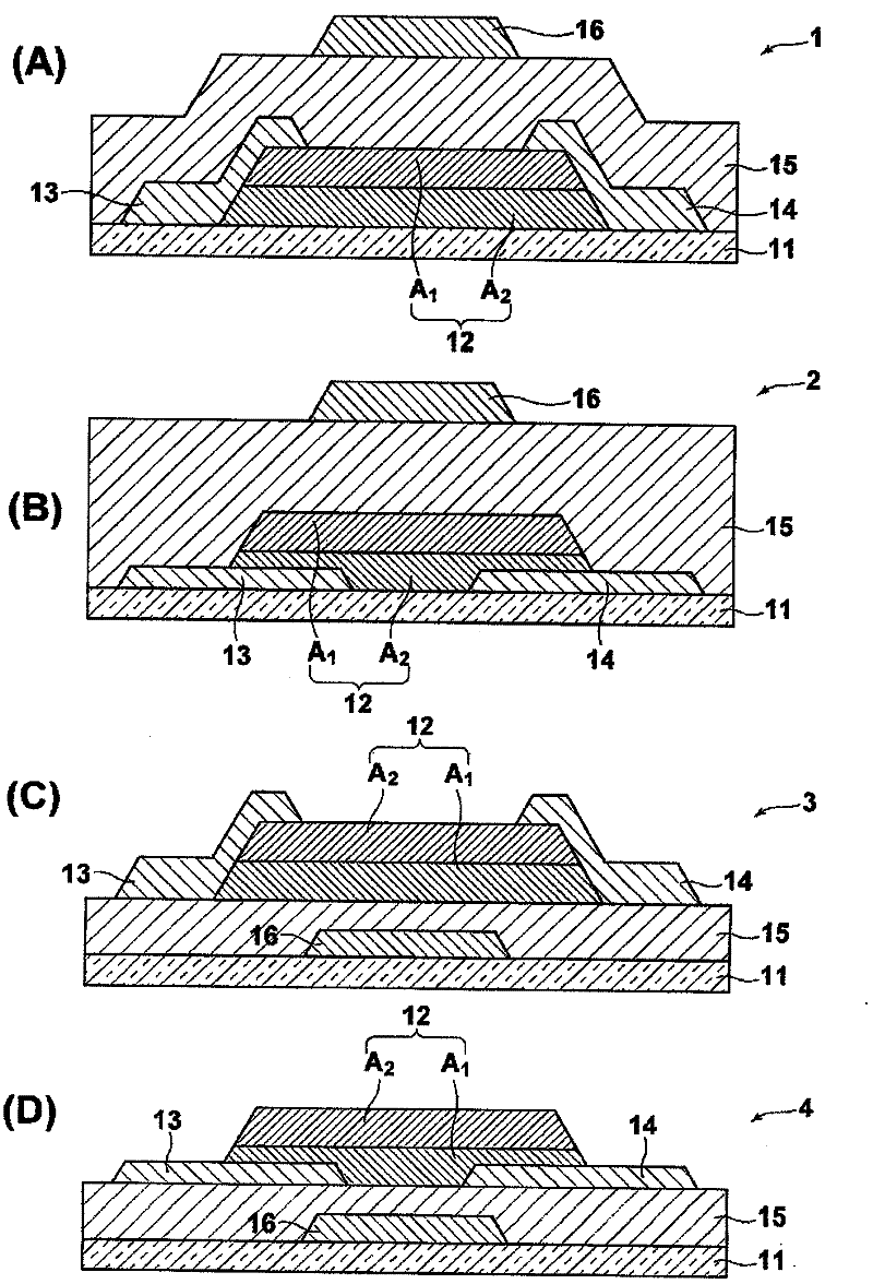
[0216] As Example 1, bottom-gate and top-gate thin film transistors were produced. As the substrate, SiO with 100nm formed on the surface is used 2 A p-type silicon substrate (manufactured by Mitsubishi Materials Corporation) doped with a high concentration of an oxide film. The oxide semiconductor layer is made of a material composed of IGZO. First, as the first region A 1 After sputtering a 5nm InGaZnO film with Ga / (In+Ga)=0.25 and Zn / (In+Ga)=0.5, the second region A 2 A 30 nm IGZO film of Ga / (In+Ga)=0.75 and Zn / (In+Ga)=0.5 was formed by sputtering. The oxide semiconductor layer is formed continuously between regions without being exposed to t...

Embodiment 2

[0232] The element configuration is the same as in Example 1, and only the composition of the oxide semiconductor layer is different. First, as the first area A 1After sputtering a 5nm IGZO film with Ga / (In+Ga)=0.375 and Zn / (In+Ga)=0.5, the second region A 2 A 30 nm IGZO film of Ga / (In+Ga)=0.625 and Zn / (In+Ga)=0.5 was formed by sputtering. The oxide semiconductor layer is formed continuously between regions without being exposed to the atmosphere. The sputtering of each area is based on the use of In 2 o 3 Target, Ga 2 o 3 Target, ZnO target co-sputtering (co-sputter) carried out. The adjustment of the film thickness of each region is performed by adjusting the film formation time. The detailed sputtering conditions of each region are as follows.

[0233] (first area A 1 sputtering conditions)

[0234] Achieved vacuum degree: 6×10 -6 Pa

[0235] Film forming pressure: 4.4×10 -1 Pa

[0236] Film forming temperature: room temperature

[0237] Oxygen partial pressu...

Embodiment 3

[0246] The device configuration is the same as in Example 1, but the composition and oxygen concentration of the oxide semiconductor layer are different. First, as the first area A 1 After sputtering and forming a 5nm IGZO film with Ga / (In+Ga)=0.0 and Zn / (In+Ga)=0.5, the second region A 2 A 30 nm IGZO film of Ga / (In+Ga)=1.0 and Zn / (In+Ga)=0.5 was formed by sputtering. The oxide semiconductor layer is formed continuously between regions without being exposed to the atmosphere. The sputtering of each area is based on the use of In 2 o 3 Target, Ga 2 o 3 Target, ZnO target co-sputtering (co-sputter) carried out. The adjustment of the film thickness of each region is performed by adjusting the film formation time. The detailed sputtering conditions of each region are as follows.

[0247] (first area A 1 sputtering conditions)

[0248] Achieved vacuum degree: 6×10 -6 Pa

[0249] Film forming pressure: 4.4×10 -1 Pa

[0250] Film forming temperature: room temperature

...


PUM


Abstract

Provided is a thin film transistor which can be made at a low temperature and display high field effect mobility. The thin film transistor comprises an active layer having oxide semiconductor layer. The active layer (12) comprises a first area A1 having a first electronic appetency X1 along the film thickness direction from the gate electrode side and a second area A2 of the second electronic appetency X2 smaller than the first electronic appetency X1, and forms a trap type potential employing the first area A1 as the trap layer and employing the second area A2 and the gate insulating film (15) as a barrier layer. In the invention, the active layer (12) is an oxide semiconductor layer composed of a (In2O3), b (Ga2O3), and c (ZnO), thereby making the b/ (a plus b) of the second area A2 greater than b /(a plus b) of the first area A1.

Description

technical field [0001] The present invention relates to a thin film transistor including an oxide semiconductor film and a method for manufacturing the same. In addition, the present invention also relates to devices such as a display device, an image sensor, and an X-ray digital photography device using the thin film transistor. Background technique [0002] In recent years, research and development of a thin film transistor using an In-Ga-Zn-O-based (IGZO) oxide semiconductor thin film for a channel layer has been vigorously conducted. The above-mentioned oxide thin film can be formed at low temperature, exhibits higher mobility than amorphous silicon, and is transparent under visible light, so a flexible transparent thin film transistor can be formed on a substrate such as a plastic plate or film. [0003] Table 1 shows a comparative table of mobility, processing temperature, etc. of various transistor characteristics. [0004] [Table 1] [0005] [0006] Although t...

Claims


Application Information

Patent Timeline
Patent Type & Authority Applications(China)
IPC IPC(8): H01L29/786H01L29/26H01L21/363
CPCH01L21/02631H01L29/78618H01L29/7869H01L29/78696
Inventor 小野雅司高田真宏田中淳铃木真之
Owner SAMSUNG DISPLAY CO LTD
Why Eureka
Try Eureka