Ultra-wide dynamic range image sensor based on pixel charge compensation technology
An image sensor and wide dynamic range technology, applied in image communication, color TV components, TV system components, etc., can solve the problem of reducing weak light response characteristics, complex external reading and storage circuits, and reducing pixel filling ratio And other issues
- Summary
- Abstract
- Description
- Claims
- Application Information
AI Technical Summary
Problems solved by technology
Method used
Image
Examples
Embodiment 1
[0038] The image sensor of the present invention is fully compatible with the standard CMOS process. The image sensor array composed of a 320×240 area array will be described in detail below based on the 0.18 μm standard CMOS process, with reference to the drawings and embodiments.
[0039] Device system design
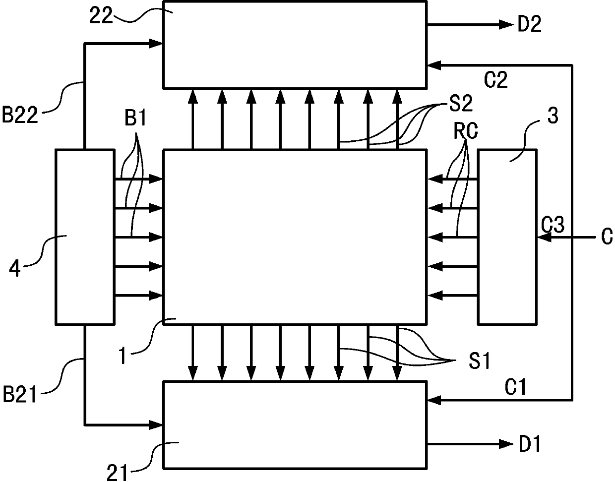
[0040] In this specific embodiment, the image sensor is designed under the standard 0.18 μm CMOS process. The system architecture adopts figure 1 structure shown. The pixel array in the designed module 1 is arranged into 240 rows and 320 columns, such as Figure 7 shown. Each pixel unit adopts such as Figure 4 In the 3T structure shown, the pixel output S1 of each column is connected to the signal bus Signal Bus. And set the current source load I on the bus Signal Bus1~SignalBus 320 of each column B1 ~ I B320 . As the light intensity changes continuously, the pixel array generates a continuously changing voltage signal. This signal is generated by the row de...
PUM
 Abstract
Description
Claims
Application Information


