Semiconductor device and making method thereof

A device manufacturing method and semiconductor technology, which are used in semiconductor/solid-state device manufacturing, semiconductor devices, electrical components, etc., can solve the problems of limited overall device performance improvement, inability to take into account power consumption and reduce driving ability, etc., to improve the on-state current. Effect

Active Publication Date: 2014-02-19
INST OF MICROELECTRONICS CHINESE ACAD OF SCI
View PDF3 Cites 19 Cited by
  • Summary
  • Abstract
  • Description
  • Claims
  • Application Information

AI Technical Summary

Problems solved by technology

However, when the size continues to shrink below 22nm, the driving current of the existing ordinary TFET is 3 to 4 orders of magnitude lower than that of the conventional MOSFET, which makes it impossible to take into account the reduction of power consumption and the improvement of driving capability, and the overall performance of the device is limited.

Method used


Image

  • Semiconductor device and making method thereof
  • Semiconductor device and making method thereof
  • Semiconductor device and making method thereof

Examples


Embodiment Construction

[0033] The features and technical effects of the technical solution of the present invention will be described in detail below with reference to the accompanying drawings and in combination with exemplary embodiments. It should be pointed out that similar reference numerals represent similar structures, and the terms "first", "second", "upper", "lower", "thick", "thin" and the like used in this application can be used for Modify various device structures. These modifications do not imply a spatial, sequential or hierarchical relationship of the modified device structures unless specifically stated.

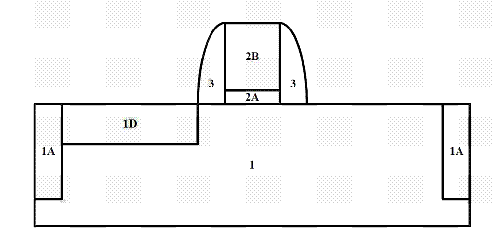
[0034] According to the first embodiment of the present invention, refer to Figure 1 to Figure 3 , forming a conventional MOSFET device structure with GeSn stressed source and drain regions.

[0035] First refer to figure 1 A gate stack structure 2 and a gate spacer 3 are formed on the substrate 1 , and a drain region 1D is formed by implanting into the substrate 1 on one side...


PUM

PropertyMeasurementUnit
depthaaaaaaaaaa
thicknessaaaaaaaaaa

Abstract

A semiconductor device is disclosed, and comprises a substrate, a gate stack structure on the substrate, source/drain regions in the substrate at two sides of the gate stack structure, and a channel region between the source/drain regions in the substrate. The source region in the source/drain region comprises a GeSn alloy, and a tunneling dielectric layer optionally exists between the GeSn alloy of the source region and the channel region. By using the semiconductor device and a manufacturing method thereof in the present invention, selective epitaxy is performed, or a precursor is injected and then rapid annealing is performed through laser, to form a GeSn alloy with a narrow band gap, thereby effectively increasing an on-state current of a TFET, and having an important application prospect in a high-performance low-consumption application.

Description

technical field [0001] The invention relates to the field of semiconductor integrated circuit manufacturing, more specifically, to a tunneling field effect transistor (TFET) with a GeSn alloy as a source and a manufacturing method thereof. Background technique [0002] With the continuous development of integrated circuit technology, especially the continuous proportional reduction of device size, various key parameters of the device, such as threshold voltage, have also been reduced. The advantages of reduced power consumption and improved integration have promoted the overall performance of the device. However, at the same time, the driving capability of the device is limited by the traditional silicon material process, the carrier mobility is low, and the driving capability of the device is relatively insufficient. Therefore, high-mobility channel devices have an important application background in the future. [0003] Existing high-mobility channel devices are usually m...

Claims


Application Information

Patent Timeline
Patent Type & Authority Applications(China)
IPC IPC(8): H01L29/161H01L29/739H01L21/268H01L21/331
CPCH01L21/26506H01L21/268H01L29/0895H01L29/165H01L29/66636H01L29/66643H01L29/66659H01L29/7848H01L29/7391H01L29/0847H01L29/161H01L29/66356
Inventor 马小龙殷华湘付作振
Owner INST OF MICROELECTRONICS CHINESE ACAD OF SCI
Why Eureka
Try Eureka