Nor Flash chip control method based on AXI bus
A control method and chip technology, applied in instruments, electrical digital data processing, etc., can solve problems such as low data throughput, complex AHB bus, and difficulty in optimizing individual channels, and achieve high practical value, simple structure, and good compatibility. Effect
- Summary
- Abstract
- Description
- Claims
- Application Information
AI Technical Summary
Problems solved by technology
Method used
Image

Examples
Embodiment
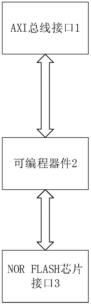
[0023] Examples of the present invention figure 1 As shown, a control method of a Nor Flash chip based on the AXI bus is realized by the following system, the system includes an AXI bus interface 1, a programmable device 2 and a Nor Flash chip interface 3, an AXI bus interface 1 and a programmable device 2 Connection, the programmable device 2 is connected with the Nor Flash chip interface 3; the AXI bus interface 1 is connected with the SOC system, and the Nor Flash chip interface 3 is connected with the Nor Flash chip; the programmable device 2 is used to receive and process the information transmitted by the AXI bus, press It is required to control the reading and writing of the Nor Flash chip, so as to realize the communication between the AXI bus and the Nor Flash chip. In the process of connecting the circuit between the AXI bus and the Nor Flash chip, the programmable device 2 receives the information sent by the SOC system through the AXI bus interface 1, and Decode th...
PUM
 Abstract
Description
Claims
Application Information