Optimizing method for integrated circuit clock grid driving based on driving window

A clock grid, integrated circuit technology, applied in electrical digital data processing, special data processing applications, instruments, etc., can solve the problems of difficult timing convergence, poor layout, wiring congestion, etc., to achieve good scalability and save chips The effect of area occupancy

Active Publication Date: 2016-06-22
NAT UNIV OF DEFENSE TECH
View PDF4 Cites 0 Cited by
  • Summary
  • Abstract
  • Description
  • Claims
  • Application Information

AI Technical Summary

Problems solved by technology

In today's large-scale chip design, there are often a series of negative effects such as wiring congestion caused by driver unit congestion, difficulty in timing convergence, excessive local voltage drop, and excessive local power consumption density. Inappropriate choice of type is also an important reason

Method used


Image

  • Optimizing method for integrated circuit clock grid driving based on driving window
  • Optimizing method for integrated circuit clock grid driving based on driving window
  • Optimizing method for integrated circuit clock grid driving based on driving window

Examples


Embodiment Construction

[0023] Such as Figure 4 As shown, the implementation steps of the integrated circuit clock grid driving optimization method based on the driving window in this embodiment are as follows:

[0024] 1) Based on the low-pass filtering characteristics, the clock grid of the integrated circuit is divided into multiple driver windows according to the influence range of each driver, and one driver window is taken as the current driver window, and then jump to step 2).

[0025] In this embodiment, the driving window obtained by separating the clock grid of the integrated circuit is a rectangular window, and each main intersection point of the clock grid is located at the center of the rectangular window, specifically as follows Figure 5 As shown in , the triangles in the figure represent the drivers placed at the intersections of the backbones of the grid, and each rectangular area represents the influence range of the corresponding driver—the driving window, and the small black dots...


PUM


Abstract

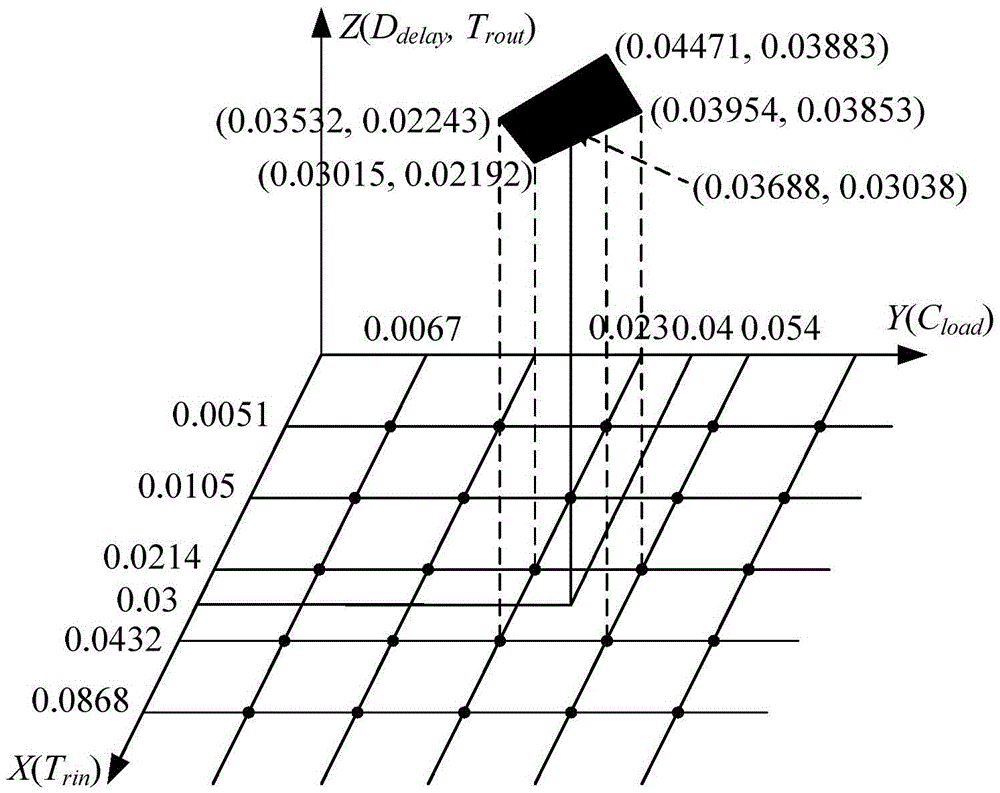
The invention discloses a drive window-based integrated circuit clock grid drive optimization method, the implementation steps of which are as follows: divide the clock grid into multiple drive windows according to the influence range of each driver based on the low-pass filter characteristics, and traverse the drive windows , for each current drive window that is traversed, estimate the load capacitance in the current drive window, and perform bilinear interpolation look-up table to calculate all alternative drivers according to the typical input signal transition time and load capacitance under the current process. The device delay and output signal transition time; sequentially select the unit that is not greater than the maximum transition time specified by the user, the device delay is within the user-specified range, and the smallest area is used as the driver of the current drive window to complete the clock grid drive optimization. . The invention can ensure that the grid is driven reasonably without causing excessive drive, saves chip area occupation, has strong scalability, and can be conveniently combined with other grid optimization strategies.

Description

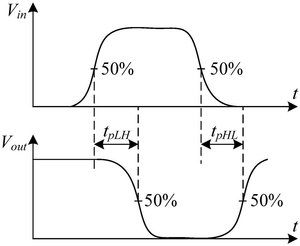
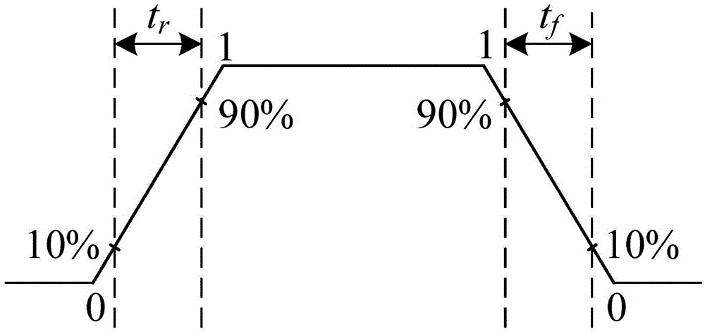
technical field [0001] The present invention relates to the field of integrated circuit (Integrated Circuit, hereinafter referred to as IC) design automation of microelectronics technology, and in particular to an integrated circuit clock grid drive optimization method based on a drive window. Background technique [0002] In the physical design of semi-custom integrated circuits, devices are basically selected from the cell library provided by the process manufacturer, so the timing and physical indicators of the cells need to be specially considered to meet various design requirements. The timing of the device mainly refers to the device delay and the output signal transition time, and the physical index of the device mainly concerns the size of the unit area. [0003] The device delay indicates the time elapsed when the signal passes through a logic gate. Generally, it is defined as the time required for a 50% change in the input signal voltage to a 50% change in the outp...

Claims


Application Information

Patent Timeline
Patent Type & Authority Patents(China)
IPC IPC(8): G06F17/50
Inventor 乐大珩杨正强赵振宇窦强何小威马驰远冯超超余金山马卓
Owner NAT UNIV OF DEFENSE TECH
Why Eureka
Try Eureka