Method for removing noise in level signals

A technology of level signals and glitches, applied in the directions of generating/distributing signals, pulse shaping, etc., can solve the problem of reducing the working speed of the chip, and achieve the effect of less chip area overhead, ensuring correctness, and improving reliability.

Active Publication Date: 2014-03-12
SHANGHAI HUAHONG INTEGRATED CIRCUIT
View PDF2 Cites 4 Cited by
  • Summary
  • Abstract
  • Description
  • Claims
  • Application Information

AI Technical Summary

Problems solved by technology

When this type of operation is dominant in the chi

Method used


Image

  • Method for removing noise in level signals
  • Method for removing noise in level signals
  • Method for removing noise in level signals

Examples


Embodiment Construction

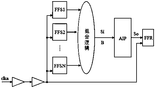
[0014] Asynchronous analog modules have relatively high requirements for input signals, no glitches, and clean level signals. In combinational logic, because part of the input changes simultaneously in a very short time, the output of the combinational logic has glitches. The asynchronous signal interface is sensitive to glitches and affects the correctness of the function; therefore, it is very important to filter glitches.

[0015] Such as figure 1 As shown, assuming that there is an input clock domain clka in the design, the output signal Si of the combinational logic is composed of the output signals of several input registers FFS1~FFSN belonging to the combinational logic of the input clock domain clka, and for the asynchronous analog module AIP It is an asynchronous signal. Assume that the input clock domain clka inputs data into the input registers FFS1~FFSN of the combinational logic at the rising edge of the nth clock cycle, and generates the output signal Si of the comb...


PUM


Abstract

The invention discloses a method for removing noise in level signals. The method includes the following steps that step1, input signals of a concerned asynchronous analog module are found; step2, the source of the input signals is traced, and whether the source is formed by combinatorial logic or not and whether multiple signals change simultaneously or not are judged; step3, the maximum time delay Ddm of the combinatorial logic is calculated; step4, a noise removing register is set, the data input end D of the noise removing register is connected with the output end of the combinatorial logic, the output end Q of the noise removing register is connected with the input end of the asynchronous analog module, the clock end uses a clock with the same clock domain as the asynchronous analog module, and the difference between the clock time delay Dce of an input register of the combinatorial logic and the time delay Dcs of the noise removing register is increased to perform delay sampling. On the premise that an interface sequential relationship is not changed, the noise of the signals can be removed through the registers so that functional stability of the asynchronous analog module can be ensured.

Description

Technical field [0001] The invention relates to a method for removing burrs in level signals. Background technique [0002] As chip functions become more and more complex, more and more designs will use complex analog modules, such as memory. These analog modules have stricter requirements for certain input signals, especially asynchronous analog signals, and there must be no glitches, otherwise they will cause incorrect functions. The general method to eliminate glitches is to use register output, that is, use the signal output from the register to directly drive the asynchronous signal of the analog module, which requires a timing delay of one clock cycle. When this type of operation dominates the chip, the working speed of the chip is greatly reduced. How to provide clean level signals to asynchronous analog modules while ensuring the working speed of the chip is one of the main problems in circuit design. Summary of the invention [0003] The technical problem to be solved ...

Claims


Application Information

Patent Timeline
IPC IPC(8): G06F1/04H03K5/01
Inventor 王永流张伸
Owner SHANGHAI HUAHONG INTEGRATED CIRCUIT
Why Eureka
Try Eureka