Electronic component mounting system, electronic component mounting apparatus and electronic component mounting method

A technology for electronic parts and installation systems, which is applied in the direction of assembling printed circuits, electrical components, and electrical components with electrical components, which can solve the problems of difficulty in ensuring printing position accuracy, increase in manufacturing costs, and difficulty in obtaining position correction effects, and achieve good installation. Position accuracy, the effect of securing the installation position accuracy

Active Publication Date: 2014-03-12
PANASONIC INTELLECTUAL PROPERTY MANAGEMENT CO LTD
View PDF3 Cites 2 Cited by
  • Summary
  • Abstract
  • Description
  • Claims
  • Application Information

AI Technical Summary

Problems solved by technology

In reality, however, the target position to be printed with solder is the opening of the resist film, so when the position of the opening on the electrode surface deviates from the center of the electrode, the position information of the electrode is directly fed forward as described above. In the way, it is difficult to obtain the desired position correction effect
In addition, if the accuracy of the formation position of the resist film is to be improved, the film formation process is complicated and the production cost is greatly increased.
In this way, in the prior art, when a substrate in which the protective film is formed in a range other than the openings set in the electrodes is targeted, there is a problem that it is difficult to ensure good printing position accuracy.

Method used


Image

  • Electronic component mounting system, electronic component mounting apparatus and electronic component mounting method
  • Electronic component mounting system, electronic component mounting apparatus and electronic component mounting method
  • Electronic component mounting system, electronic component mounting apparatus and electronic component mounting method

Examples


Embodiment Construction

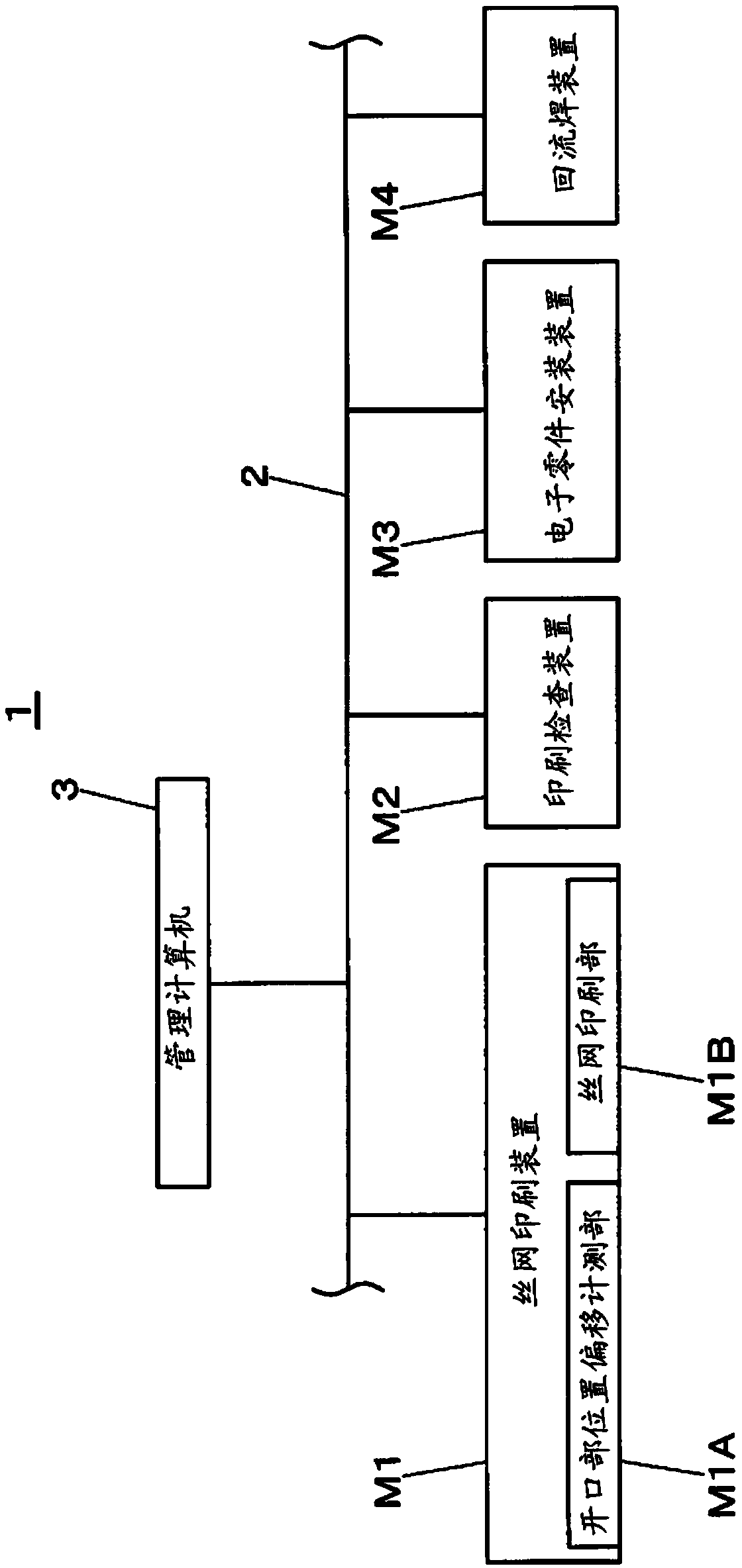
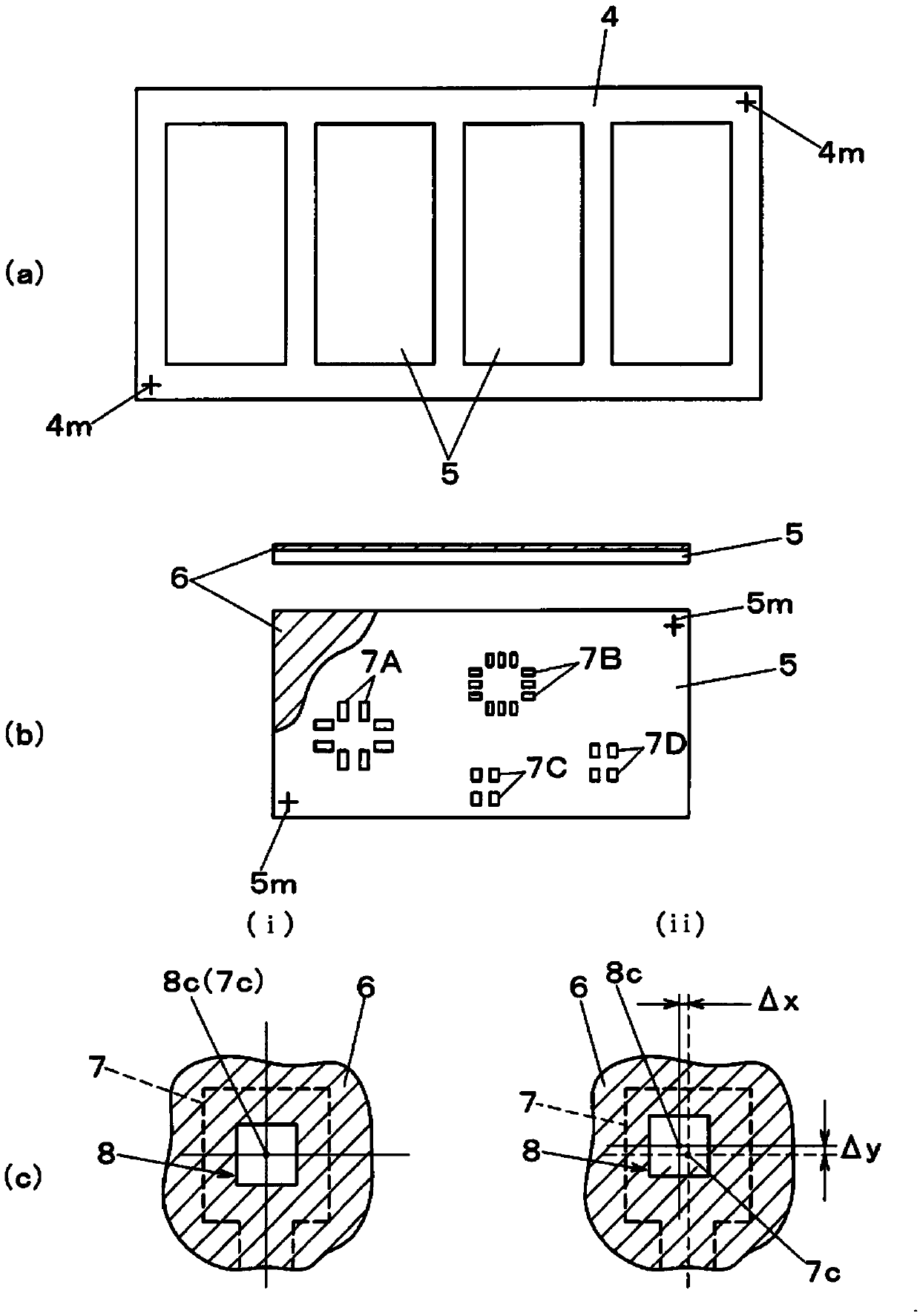
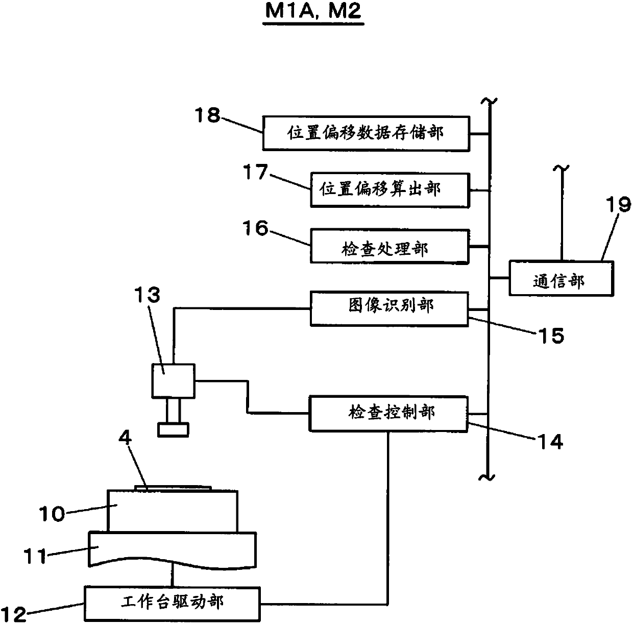
[0031] Hereinafter, embodiments of the present invention will be described with reference to the drawings. First, refer to figure 1 The configuration of the electronic component mounting system 1 having a function of manufacturing a mounted substrate by mounting electronic components on the substrate by soldering will be described. exist figure 1 Among them, the electronic component installation system 1 adopts the configuration that the electronic component installation line is connected through the communication network 2, and is controlled by the management computer 3. The electronic component installation line connects the screen printing device M1, the printing inspection device M2, the electronic The component mounting device M3, the reflow soldering device M4 and other devices are connected together.

[0032]The screen printing apparatus M1 screen-prints cream solder (cream solder) for bonding electronic components on a substrate to be processed. The printing inspect...


PUM


Abstract

The invention provides an electronic component mounting system, an electronic component mounting apparatus and an electronic component mounting method, wherein except the part to be formed as the opening part of an electrode, the other part of a substrate is covered with a protective film. With the above substrate as a target, the printing is ensured to be good in position accuracy. Before the solder printing process, an opening part (8) is optically identified. Meanwhile, the opening position offset between the standard position of the electrode (7) and the actual position of the opening part (8) is stored. Furthermore, with the position of the opening part (8) as a target position, the solder (S) is printed. After that, the printed solder (S) is optically identified. Meanwhile, the solder position offset between the position of the solder (S) and the position of the opening part (8) is stored. During the installation control process, a component mounting mechanism controls a mounting head to transfer electronic components to a single substrate (5). Meanwhile, based on the above opening position offset and the solder position offset, the component mounting mechanism is controlled in such as a way that electronic components (9) are landed in an installation position between the centre-of-gravity position (8*) of the opening part (8) and the centre-of-gravity position (S*) of the printed solder.

Description

technical field [0001] The present invention relates to an electronic component mounting system for manufacturing a mounted substrate by mounting electronic components on a substrate by soldering, an electronic component mounting device and an electronic component mounting method used in the electronic component mounting system. Background technique [0002] Along with the miniaturization of electronic equipment, the mounting density of circuit boards is also increasing, and the positional accuracy when mounting electronic components on the electrodes for electronic component bonding on the substrate is also becoming more refined. In order to cope with such high mounting position accuracy, a feed-forward method is introduced that measures the electrode position error that occurs when electrodes are formed on the board and the printing position of the solder printed on the electrodes for each board. errors, and then transmit the error information to the post-process equipment...

Claims


Application Information

Patent Timeline
Patent Type & Authority Applications(China)
IPC IPC(8): H05K13/04H05K3/34
Inventor 友松道范池田政典八朔阳介
Owner PANASONIC INTELLECTUAL PROPERTY MANAGEMENT CO LTD
Why Eureka
Try Eureka