OGS touch screen and manufacturing method thereof

A production method and touch screen technology, which are applied in the fields of instruments, electrical digital data processing, and data processing input/output processes, etc., can solve problems such as hardness not meeting customer requirements, many times of glass layer strengthening, affecting the service life of the whole machine, etc. , to achieve the effect that the line is not easy to break, the yield is high, and the production cost is low.

Inactive Publication Date: 2014-03-19
金振平 +2
View PDF5 Cites 12 Cited by
  • Summary
  • Abstract
  • Description
  • Claims
  • Application Information

AI Technical Summary

Problems solved by technology

However, in practical applications, the existing touch screen has the disadvantage of being easily broken, which affects the service life of the whole machine. The reason is that the existing touch screen is mainly composed of a panel, a conductive plate, and glass with multi-layer circuit printing layers printed on the upper surface. Composition, and glass is the main reason why existing touch screens are easily broken
The thickness of direct printing on the surface of the glass layer is too thick, the subsequent ITO and yellow lithography process, the line is easy to break, and the pass rate of good products is low. Secondly, the glass layer has been strengthened many times, and the hardness cannot meet customer needs.

Method used


Image

  • OGS touch screen and manufacturing method thereof

Examples


Embodiment 1

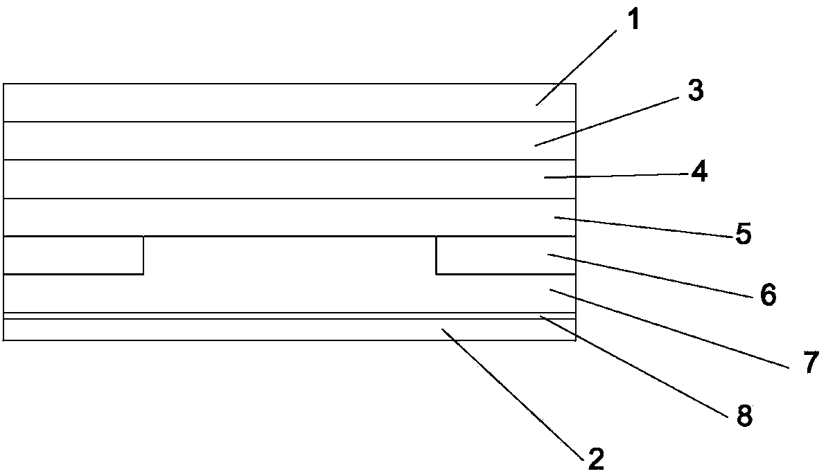
[0026] Embodiment one: if figure 1 As shown, an OGS touch screen includes an upper protective layer 1 and a lower protective layer 2, and between the upper protective layer 1 and the lower protective layer 2, a glass layer 3, an optical adhesive layer 4, and an optical grade PET layer are sequentially arranged from top to bottom. 5. The three-layer ink layer 6 and the printing surface are coated with a transparent conductive layer 7, and the printing surface is coated with a layer of photoresist layer 8.

[0027] In the meantime, the thickness of the glass layer 3 used in this embodiment is 0.7mm.

[0028] The thickness of the optical adhesive layer 4 used in this embodiment is 0.025 mm.

[0029] The optical grade PET layer 5 used in this embodiment has a thickness of 0.125mm.

[0030] The ink layer 6 used in this embodiment has a thickness of 0.013mm.

[0031] The upper protective layer 1 and the lower protective layer 2 used in this embodiment have a thickness of 0.05 mm....

Embodiment 2

[0033] Embodiment two: if figure 1 As shown, an OGS touch screen includes an upper protective layer 1 and a lower protective layer 2, and between the upper protective layer 1 and the lower protective layer 2, a glass layer 3, an optical adhesive layer 4, and an optical grade PET layer are sequentially arranged from top to bottom. 5. Four layers of ink layer 6 and the whole surface are plated with a transparent conductive layer 7, and the whole surface is coated with a layer of photoresist layer 8 on the lower surface of the transparent conductive layer 7.

[0034] In the meantime, the thickness of the glass layer 3 used in this embodiment is 0.8 mm.

[0035] The optical adhesive layer 4 used in this embodiment has a thickness of 0.1 mm.

[0036] The optical grade PET layer 5 used in this embodiment has a thickness of 0.08 mm.

[0037] The ink layer 6 used in this embodiment has a thickness of 0.01 mm.

[0038] The upper protective layer 1 and the lower protective layer 2 us...

Embodiment 3

[0040] Embodiment three: as figure 1 As shown, an OGS touch screen includes an upper protective layer 1 and a lower protective layer 2, and between the upper protective layer 1 and the lower protective layer 2, a glass layer 3, an optical adhesive layer 4, and an optical grade PET layer are sequentially arranged from top to bottom. 5. Five layers of ink layer 6 and the whole surface are plated with a transparent conductive layer 7, and the lower surface of the whole surface is coated with a layer of photoresist layer 8.

[0041] In the meantime, the thickness of the glass layer 3 used in this embodiment is 1.5 mm.

[0042] The thickness of the optical adhesive layer 4 used in this embodiment is 0.2 mm.

[0043] The optical grade PET layer 5 used in this embodiment has a thickness of 0.15 mm.

[0044] The ink layer 6 used in this embodiment has a thickness of 0.04mm.

[0045] The upper protective layer 1 and the lower protective layer 2 used in this embodiment have a thickne...


PUM


Abstract

The invention discloses an OGS touch screen and a manufacturing method of the OGS touch screen. The OGS touch screen comprises an upper protective layer and a lower protective layer. A glass layer, an optical glue layer, an optical-level PET layer, multiple ink layers and a printing face whole-face-plated transparent conductive layer are sequentially arranged between the upper protective layer and the lower protective layer from top to bottom. The printing face of the whole-face-plated transparent conductive layer is coated with a photoresistance layer. According to the OGS touch screen, the tempered glass layer and an optical-level PET substrate are adopted, the glass layer and the optical-level PET layer adhere to each other through the optical glue layer, the ink layers are printed on the printing face of the optical-level PET layer, and the outer surface of the glass layer and the outer surface of the printing face whole-face-plated transparent conductive layer are respectively provided with a protective film so that the whole product can be protected; the surface of the printing face whole-face-plated transparent conductive layer is coated with the photoresistance layer so that the photoresist surfaces are irradiated by ultraviolet rays through the films and a conductive layer circuit can be formed on the printing face whole-face-plated transparent conductive layer.

Description

technical field [0001] The invention relates to the field of touch screens, in particular to an OGS touch screen and a manufacturing method thereof. Background technique [0002] As the latest human-computer interaction technology, touch screen is a transparent input system and an absolute positioning system. Its products are used in mobile phones, consulting appliances, industrial control instruments, vehicle-mounted GPS terminals, public consultation systems, automatic sales systems, etc. . Users only need to lightly touch the icons or text on the display screen with their fingers or electronic pen to realize the operation, thus getting rid of the dependence on the keyboard and mouse and making the human-computer interaction more straightforward. However, in practical applications, the existing touch screen has the disadvantage of being easily broken, which affects the service life of the whole machine. The reason is that the existing touch screen is mainly composed of a ...

Claims


Application Information

Patent Timeline
Patent Type & Authority Applications(China)
IPC IPC(8): G06F3/041
Inventor 金振平白孝贵罗斌玮
Owner 金振平
Why Eureka
Try Eureka