Secondary plating-prior-to-etching metal frame subtraction imbedded chip normal-installation bump structure and process method

A technology of first plating and then etching, bump structure, applied in electrical components, electric solid devices, circuits, etc., can solve the problem of lack of system functions of metal lead frames, improve heat dissipation, reduce costs, and avoid signal transmission.

Active Publication Date: 2014-03-19
JCET GROUP CO LTD
View PDF4 Cites 4 Cited by
  • Summary
  • Abstract
  • Description
  • Claims
  • Application Information

AI Technical Summary

Problems solved by technology

[0009] The purpose of the present invention is to overcome the above-mentioned shortcomings, and provide a kind of bump structure and process method of the metal frame subtraction embedded chip after the second plating, which can solve the problem of the lack of system function of the traditional metal lead frame

Method used


Image

  • Secondary plating-prior-to-etching metal frame subtraction imbedded chip normal-installation bump structure and process method
  • Secondary plating-prior-to-etching metal frame subtraction imbedded chip normal-installation bump structure and process method
  • Secondary plating-prior-to-etching metal frame subtraction imbedded chip normal-installation bump structure and process method

Examples


Embodiment Construction

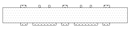
[0080] see Figure 22 , the present invention is a metal frame subtractive embedded chip bump structure after secondary plating, which includes a metal substrate frame 1, a base island 2 and pins 3 are arranged inside the metal substrate frame 1, and the pins 3 In a stepped shape, the front of the base island 2 and the pin 3 are flush with the front of the metal substrate frame 1, the back of the pin 3 is flush with the back of the metal substrate frame 1, and the back of the base island 2 is flush with the pin 3 is flush with the stepped surface, the stepped surface of the pin 3 is provided with a metal layer 4, the back of the base island 2 is equipped with a chip 6 through a conductive or non-conductive adhesive substance 5, and the surface of the chip 6 is connected to the metal layer. The surfaces of 4 are connected by metal wires 7, and the inner area of ​​the metal substrate frame 1 is filled with a molding compound 8, the front of the molding compound 8 is flush with t...


PUM


Abstract

The invention relates to a secondary plating-prior-to-etching metal frame subtraction imbedded chip normal-installation bump structure and a process method. The structure comprises a metal substrate fame (1). The metal substrate fame (1) is internally provided with base islands (2) and pins (3). The back surface of each base island (2) is flush with the step surface of each pin (3). The step surface of each pin (3) is provided with a metal layer (4). The back surface of each base island (2) is normally equipped with a chip (6). The surface of the chip (6) is connected with the surface of the metal layer (4) through a metal line (7). The metal substrate fame (1) is internally filled with plastic packaging material (8). The front surface of the plastic packaging material (8) is flush with the step surface of the pin (3). The back surface of the plastic packaging material (8) is flush with the back surface of the metal substrate fame (1). The front surface of the base island (2), the front surface and the back surface of each pin (3) as well as the front surface and the back surface of the metal substrate fame (1) are provided with an anti-oxidation layer (9). The back surface of each pin (3) is provided with a metal ball (10). The beneficial effect of the structure and method is that: the problem that the function and the application performance of a conventional metal lead frame are limited since an object cannot be imbedded in the metal lead frame is solved.

Description

technical field [0001] The invention relates to a bump structure and a process method of a front-mounted bump structure and a process method of a metal frame subtraction embedded chip after plating first and then etching, and belongs to the technical field of semiconductor packaging. Background technique [0002] There are two main types of conventional four-sided flat leadless metal leadframe structures: [0003] One is the four-sided flat no-lead package (QFN) lead frame. The lead frame of this structure is composed of a copper metal frame and a high temperature resistant adhesive film (such as Figure 23 shown); [0004] One is the pre-encapsulated quad flat no-leads (PQFN) leadframe, the leadframe structure of this structure includes the lead and the base island, and the etched area between the lead and the base island is filled with plastic encapsulant (such as Figure 24 shown). [0005] The above conventional metal lead frame has the following disadvantages: [000...

Claims


Application Information

Patent Timeline
Patent Type & Authority Applications(China)
IPC IPC(8): H01L23/495H01L23/498H01L21/60
CPCH01L2224/48091H01L2224/73265H01L2924/00014
Inventor 梁志忠梁新夫王亚琴
Owner JCET GROUP CO LTD
Why Eureka
Try Eureka