One-time eroding-before-plating metal frame subtraction embedded chip inversely-arranged salient point structure and technological method

A technology of bump structure and process method, which is applied in the direction of electrical components, electrical solid devices, circuits, etc., can solve the problems of lack of system functions in metal lead frames, and achieve the effects of improving heat dissipation, reducing costs, and small size

Active Publication Date: 2014-03-26
JCET GROUP CO LTD
View PDF5 Cites 4 Cited by
  • Summary
  • Abstract
  • Description
  • Claims
  • Application Information

AI Technical Summary

Problems solved by technology

[0009] The purpose of the present invention is to overcome the above-mentioned shortcomings, and provide a kind of first etching and then metal-plated frame subtraction embedded chip flip-chip bump structure and process method, which can solve the problem of lack of system functions in traditional metal lead frames

Method used


Image

  • One-time eroding-before-plating metal frame subtraction embedded chip inversely-arranged salient point structure and technological method
  • One-time eroding-before-plating metal frame subtraction embedded chip inversely-arranged salient point structure and technological method
  • One-time eroding-before-plating metal frame subtraction embedded chip inversely-arranged salient point structure and technological method

Examples


Embodiment Construction

[0053] The process method of the present invention, which is etched first and then plated with a metal frame, is as follows:

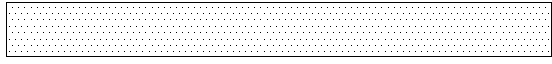
[0054] Step 1. Take the metal substrate

[0055] see figure 1 , take a piece of metal substrate with appropriate thickness, the material of this plate is mainly metal material, and the material of metal material can be copper, iron, galvanized, stainless steel, aluminum or metal that can achieve conductive function Material or non-all-metal material, etc., the choice of thickness can be selected according to product characteristics.

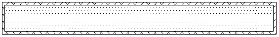
[0056] Step 2. Paste photoresist film

[0057] see figure 2 , A photoresist film that can be exposed and developed is pasted on the front and back of the metal substrate to protect the subsequent etching process. The photoresist film can be a dry photoresist film or a wet photoresist film.

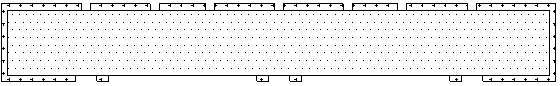
[0058] Step 3. Remove part of the photoresist film from the surface of the metal substrate

[0059] see image 3 , using exp...


PUM


Abstract

The invention relates to a one-time eroding-before-plating metal frame subtraction embedded chip inversely-arranged salient point structure and a technological method. The one-time eroding-before-plating metal frame subtraction embedded chip inverse arranged salient structure is characterized in that a metal substrate frame is included, a paddle and pins are arranged in the metal substrate frame, chips are arranged on the back face of the paddle and the step surfaces of the pins through bottom filled glue, plastic packaging materials wrap the area of the periphery of the paddle, the area between the paddle and the pins, the area between the pins, the areas on the upper portion of the paddle, the areas on the upper portions of the pins, the area on the lower portion of the paddle, and the area on the lower portions of the pins and the chips, the plastic packaging materials are aligned with the upper surface and the lower surface of the metal substrate frame, anti oxidation layers are plated on or organic solderability preservative (OSP) wraps the front face of the paddle, the front faces and the back faces of the pins and the surface of the metal substrate frame, and metal balls are arranged on the back faces of the pins. The one-time eroding-before-plating metal frame subtraction embedded chip inversely-arranged salient point structure has the advantages of being capable of solving the problem that the function and the application performance of a metal wire frame are restricted due to the fact that objects cannot be buried in the plate thickness of the traditional metal wire frame.

Description

technical field [0001] The invention relates to a flip-chip bump structure and a process method of first etching and then plating a metal frame subtractive embedded chip. It belongs to the technical field of semiconductor packaging. Background technique [0002] There are two main types of conventional four-sided flat leadless metal leadframe structures: [0003] One is the four-sided flat no-lead package (QFN) lead frame. The lead frame of this structure is composed of a copper metal frame and a high temperature resistant adhesive film (such as Figure 11 shown). [0004] One is the pre-encapsulated quad flat no-leads (pQFN) leadframe, the leadframe structure of this structure includes the lead and the base island, and the etched area between the lead and the base island is filled with plastic encapsulant (such as Figure 12 shown). [0005] The above conventional metal lead frame has the following disadvantages: [0006] 1. The traditional metal lead frame, as the pack...

Claims


Application Information

Patent Timeline
Patent Type & Authority Applications(China)
IPC IPC(8): H01L23/495H01L21/60
CPCH01L2224/73204H01L2224/16245
Inventor 梁志忠梁新夫王亚琴
Owner JCET GROUP CO LTD
Why Eureka
Try Eureka