Method for detecting planeness of PCB based on network projection

A technology of PCB board and grid projection, which is applied to measuring devices, instruments, and optical devices, etc., can solve the problems of low sensitivity, virtual welding, and high subjectivity of artificial visual detection, so as to overcome low sensitivity and high subjectivity. , Simple and accurate detection effect

Inactive Publication Date: 2014-03-26
CHINA UNIV OF MINING & TECH
View PDF6 Cites 21 Cited by
  • Summary
  • Abstract
  • Description
  • Claims
  • Application Information

AI Technical Summary

Problems solved by technology

[0002] With the rapid development of microelectronics technology, the current electronic digital products, such as mobile phones, tablet computers, notebook computers, etc., are developing in the direction of thinner and thinner. Due to the thinner and thinner requirements of product design, the components on the PCB motherboard used inside the product The density is getting higher and higher, and components with hundreds or even thousands of soldering pins are also configured on the PCB board. Devices with such a large number of pins currently use SMT surface mount technology. The flatness of the pin plane is relatively high. If the flatness of the PCB board does not meet the requirements, there will be concave and convex areas on the board surface, so that the pins will not fully contact the pads on the PCB board during soldering, resulting in empty soldering, Welding, etc., so before welding, the flatness of the PCB board needs to be tested
[0003] The current detection of PCB flatness mainly relies on manual visual inspection. This detection method is too subjective and canno

Method used


Image

  • Method for detecting planeness of PCB based on network projection
  • Method for detecting planeness of PCB based on network projection
  • Method for detecting planeness of PCB based on network projection

Examples


Embodiment Construction

[0022] The present invention will be described in detail below with reference to the accompanying drawings and in conjunction with the embodiments.

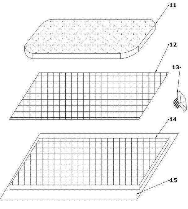
[0023] figure 1 A schematic structural view of the detection device of a preferred embodiment of the present invention is shown, including: PCB board 14 is placed on a horizontal workbench 15, a light source 11 and a baffle 12 are arranged vertically above the PCB 14, and the light source 11 is placed on the side of the baffle 12 Vertically above; the camera 13 is set at an angle of 60 degrees between the side and the horizontal workbench 15; the light source 11 projects the standard grid shadow on the baffle 12 on the PCB 14 through the baffle 12, and the camera 13 faces the The grid projection on the PCB board 14 is photographed.

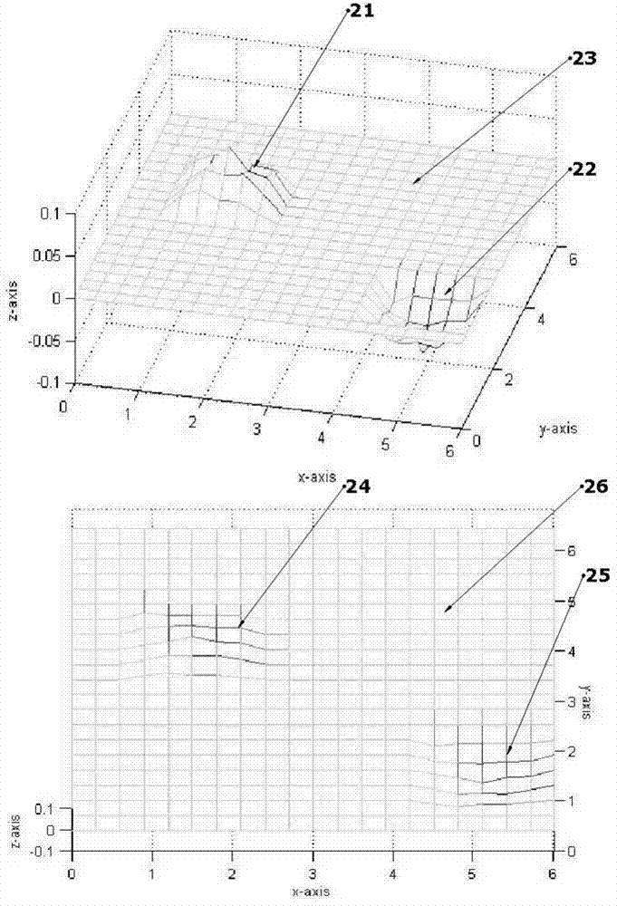
[0024] figure 2 It shows a schematic diagram of the detection principle of the preferred embodiment of the present invention, and the PCB grid shadow projection picture taken by the camera at 60 d...


PUM


Abstract

The invention provides a method for detecting the planeness of a PCB based on a network projection. The method comprises the steps that the PCB is put on a horizontal operating platform; a light source over a dam board, and the dam board are installed over the PCB; a camera is installed in an included angle of 60 degrees formed between a side and the horizontal operating platform; the light source projects the shadow of a standard grid on the dam board on the PCB by the dam board; the camera takes a picture of the shadow of the grid on the PCB from the included angle of 60 degrees. An analysis device comprising a picture processing device and a data processing device analyses the picture taken by the camera so as to decide whether the PCB meets the requirement of the planeness. The method provided by the invention simply and accurately realizes the detection of the planeness of the PCB.

Description

technical field [0001] The invention relates to the field of PCB (printed circuit board), in particular to a method for detecting the flatness of a PCB board based on grid projection. Background technique [0002] With the rapid development of microelectronics technology, the current electronic digital products, such as mobile phones, tablet computers, notebook computers, etc., are developing in the direction of thinner and thinner. Due to the thinner and thinner requirements of product design, the components on the PCB motherboard used inside the product The density is getting higher and higher, and components with hundreds or even thousands of soldering pins are also configured on the PCB board. Devices with such a large number of pins currently use SMT surface mount technology. The flatness of the pin plane is relatively high. If the flatness of the PCB board does not meet the requirements, there will be concave and convex areas on the board surface, so that the pins will...

Claims


Application Information

Patent Timeline
IPC IPC(8): G01B11/30
Inventor 陈杨梁向南亢国栋李停韩宇晨张海龙张俊升张明伟
Owner CHINA UNIV OF MINING & TECH
Why Eureka
Try Eureka