High-speed A/D sampling data real-time storage method achieved based on FPGA
A sampling data, real-time technology, applied in the direction of data acquisition and recording, can solve the problems of signal processing chip FPGA and data storage chip SRAM operating rate cannot reach such a high level, and the cost of acquisition system increases.
- Summary
- Abstract
- Description
- Claims
- Application Information
AI Technical Summary
Problems solved by technology
Method used
Image
Examples
Embodiment 1
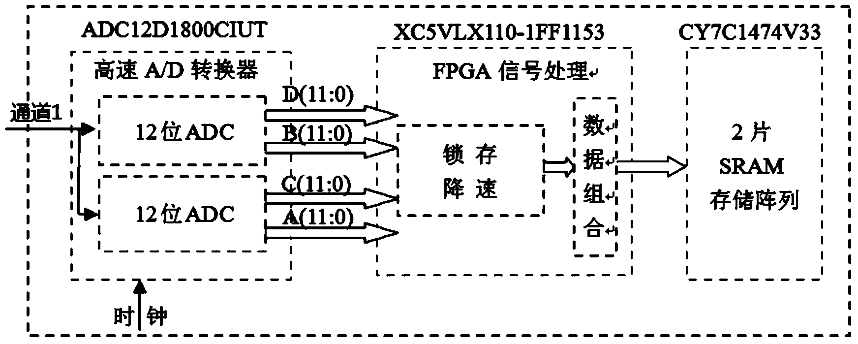
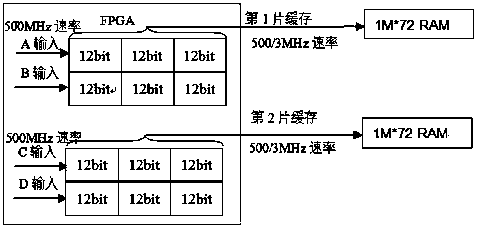
[0026] The digital signal collected at high speed is firstly processed in the FPGA, after being slowed down, combined and stored, and then transmitted to the upper-end CPU for processing through the PCI bus, so the high-speed A / D data is not lost and real-time storage is the key link of the entire acquisition system . The high-speed A / D converter used in this design is the 12-bit accuracy produced by National Semiconductor, and the sampling rate can reach 3.6GSPS. The model is ADC12D1800CIUT dual A / D core converter. Work at a sampling frequency of 2GSPS. The FPGA selected is the XC5VLX110-1FF1153 of the Virtex-5 series of XILINX Company. This type of FPGA can have a maximum of 800 available I / O ports, which can fully meet the interface connection with the high-speed A / D converter and the back-end SRAM. What SRAM chooses is Cypress Semiconductor's CY7C1474V33, its storage depth can reach 72Mbit, the data width is 72 bits, and the maximum storage rate can reach 200MHz. The FPG...
Embodiment 2
[0034] On the basis of the foregoing embodiments, further, a method for real-time storage of high-speed A / D sampling data realized based on FPGA, wherein, comprises the following steps:
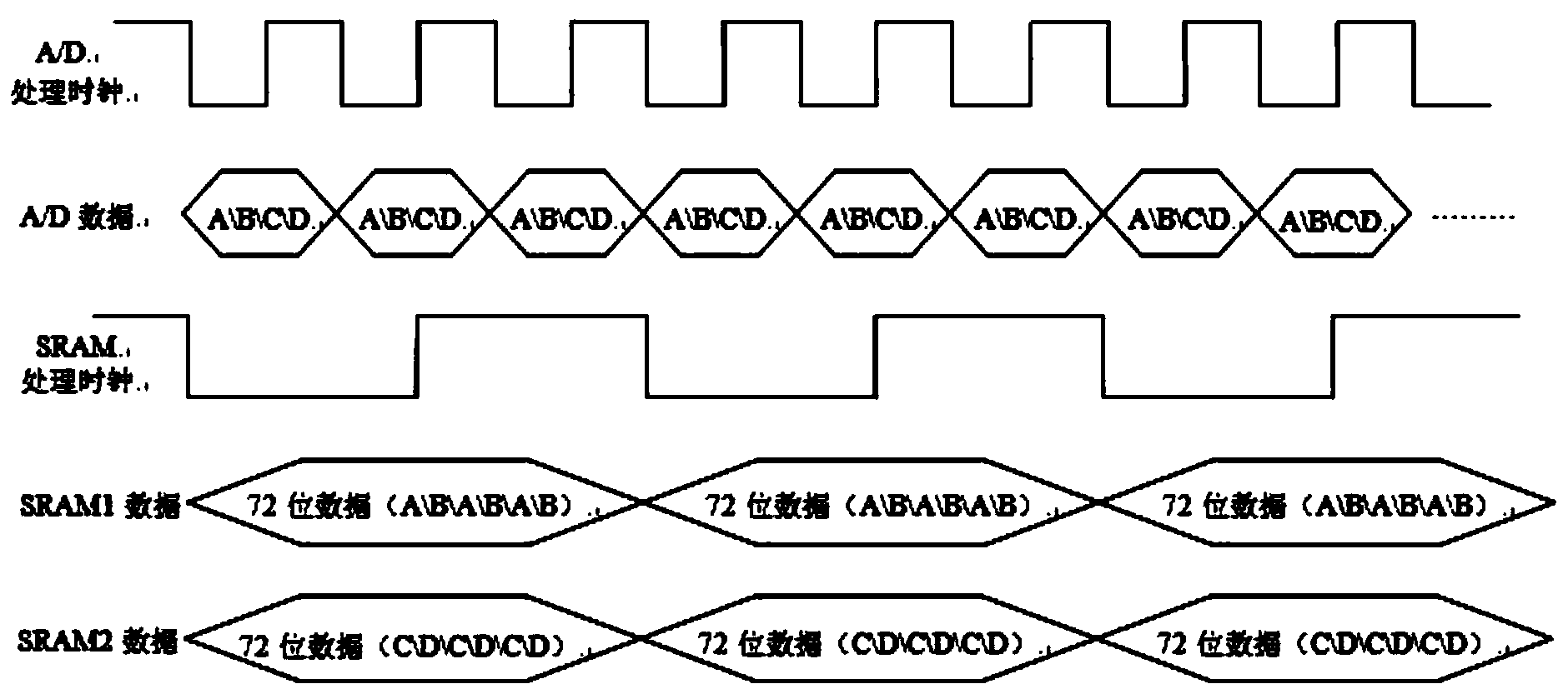
[0035] Step 1: Acquire data at the rising edge of the A / D processing clock, and convert the acquired 4-way 12-pair A / D input differential signal into a single-ended signal through the differential signal input buffer of the FPGA to form 4 groups of 12-bit data fields The A / D input data value of A / D, described 4 groups are respectively set as A, B, C, D, enter step 2;
[0036] Step 2:; judge the current input of A, B, C, D is the first input in the buffer speed reduction combination; if it is the first input, go to step 3; if it is the second input, go to step 4; if Enter step 5 for the third input;
[0037] Step 3: Write A and B into the lower 24 bits of the first SRAM temporary buffer, write C and D into the lower 24 bits of the second SRAM temporary buffer, increase the data input buffer c...
PUM
 Abstract
Description
Claims
Application Information


