Semiconductor memory device
A storage device and semiconductor technology, applied in information storage, static memory, read-only memory, etc., can solve the problem of increased deletion time
- Summary
- Abstract
- Description
- Claims
- Application Information
AI Technical Summary
Problems solved by technology
Method used
Image


Examples
no. 1 Embodiment approach
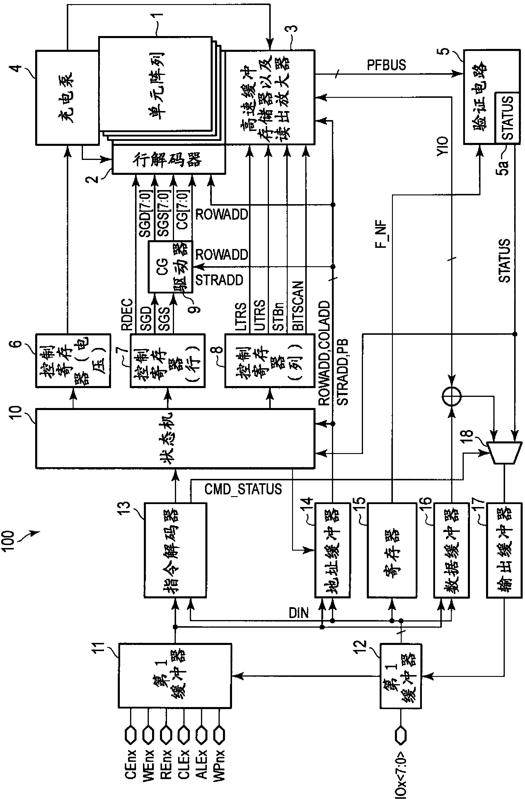
[0033] Each functional block can be realized by one of hardware, computer software, or a combination of both. Therefore, the description below will generally be made from the viewpoint of their functions to make it clear that each block is any one of the above. Whether such a function is performed as hardware or as software depends on design constraints on specific implementation forms or the entire system. Those skilled in the art can use various methods to realize these functions in each specific implementation form, but each implementation method is included in the category of the implementation manner. In addition, it is not necessary to distinguish each functional block as in the following specific examples. For example, some functions may be performed by other functional blocks than those illustrated in the following description. Furthermore, the illustrated functional blocks may be divided into finer functional sub-blocks. Which functional block is specified does not...
no. 2 Embodiment approach
[0084] In the first embodiment, the number of failed bits is counted for each string. On the other hand, in the second embodiment, the number of failed bits accumulated in all strings is counted.
[0085] Figure 13 It is a block diagram of the semiconductor memory device of the second embodiment. Figure 13 Based on the first embodiment ( figure 1 ),right figure 1 Several elements were added. like Figure 13 As shown, the register 15 also holds two thresholds F_BSPF and F_BSPF_ACCU, and outputs signals F_BSPF and F_BSPF_ACCU representing them respectively. The signals F_BSPF, F_BSPF_ACCU are received by the selection circuit 19 . The selection circuit 19 outputs one of the signals F_BSPF and F_BSPF_ACCU as the signal F_NF under the control of the state machine 10 . The signal F_NF is received by the verification circuit 5 as in the first embodiment. The threshold F_BSPF is the same as the threshold indicated by the signal F_NF of the first embodiment (threshold F_NF)....
no. 3 Embodiment approach
[0115] The third embodiment relates to a semiconductor storage system including the semiconductor storage device of the second embodiment and its controller.
[0116] Figure 20 A semiconductor memory system 300 according to the third embodiment is shown. like Figure 20 As shown, the semiconductor storage system 300 includes the semiconductor storage device 100 and the controller 200 according to the second embodiment. The semiconductor memory device 100 communicates with the controller 200 .
[0117] The controller 200 includes hardware and software related to the control of the semiconductor storage device 100 . The controller 200 generates a chip enable signal CEnx, a write enable signal WEnx, a read enable signal REnx, a command latch enable signal CLEx, an address latch enable signal ALEx, and a write protect signal WPnx, and supplies these to the semiconductor storage device 100. Also, the controller 200 generates signals such as addresses, commands, and data, and ...
PUM
 Abstract
Description
Claims
Application Information
 - R&D
- Intellectual Property
- Life Sciences
- Materials
- Tech Scout
- Unparalleled Data Quality
- Higher Quality Content
- 60% Fewer Hallucinations
Browse by: Latest US Patents, China's latest patents, Technical Efficacy Thesaurus, Application Domain, Technology Topic, Popular Technical Reports.
© 2025 PatSnap. All rights reserved.Legal|Privacy policy|Modern Slavery Act Transparency Statement|Sitemap|About US| Contact US: help@patsnap.com