Double-channel transistor and preparation method for double-channel transistor

A transistor and dual-channel technology, applied in transistors, semiconductor/solid-state device manufacturing, semiconductor devices, etc., can solve problems such as electron overflow and lower device reliability

Active Publication Date: 2014-03-26
INST OF MICROELECTRONICS CHINESE ACAD OF SCI
View PDF4 Cites 18 Cited by
  • Summary
  • Abstract
  • Description
  • Claims
  • Application Information

AI Technical Summary

Problems solved by technology

[0006] The technical problem to be solved by the present invention is to provide a double-channel transistor and its preparation method to solve the problem that electron

Method used


Image

  • Double-channel transistor and preparation method for double-channel transistor
  • Double-channel transistor and preparation method for double-channel transistor
  • Double-channel transistor and preparation method for double-channel transistor

Examples


Embodiment Construction

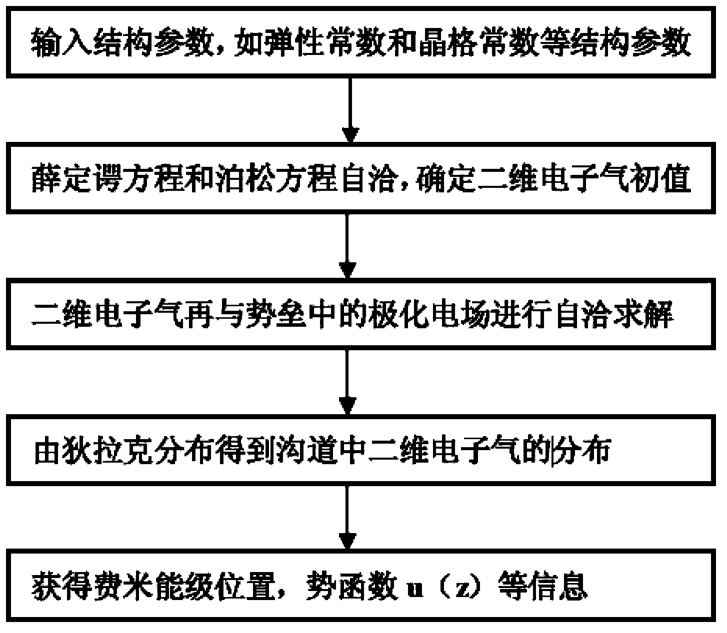
[0042] The invention provides a double-channel transistor and a preparation method thereof. In order to make the object, technical solution and advantages of the present invention clearer, the present invention will be described in further detail below in conjunction with specific embodiments and with reference to the accompanying drawings.

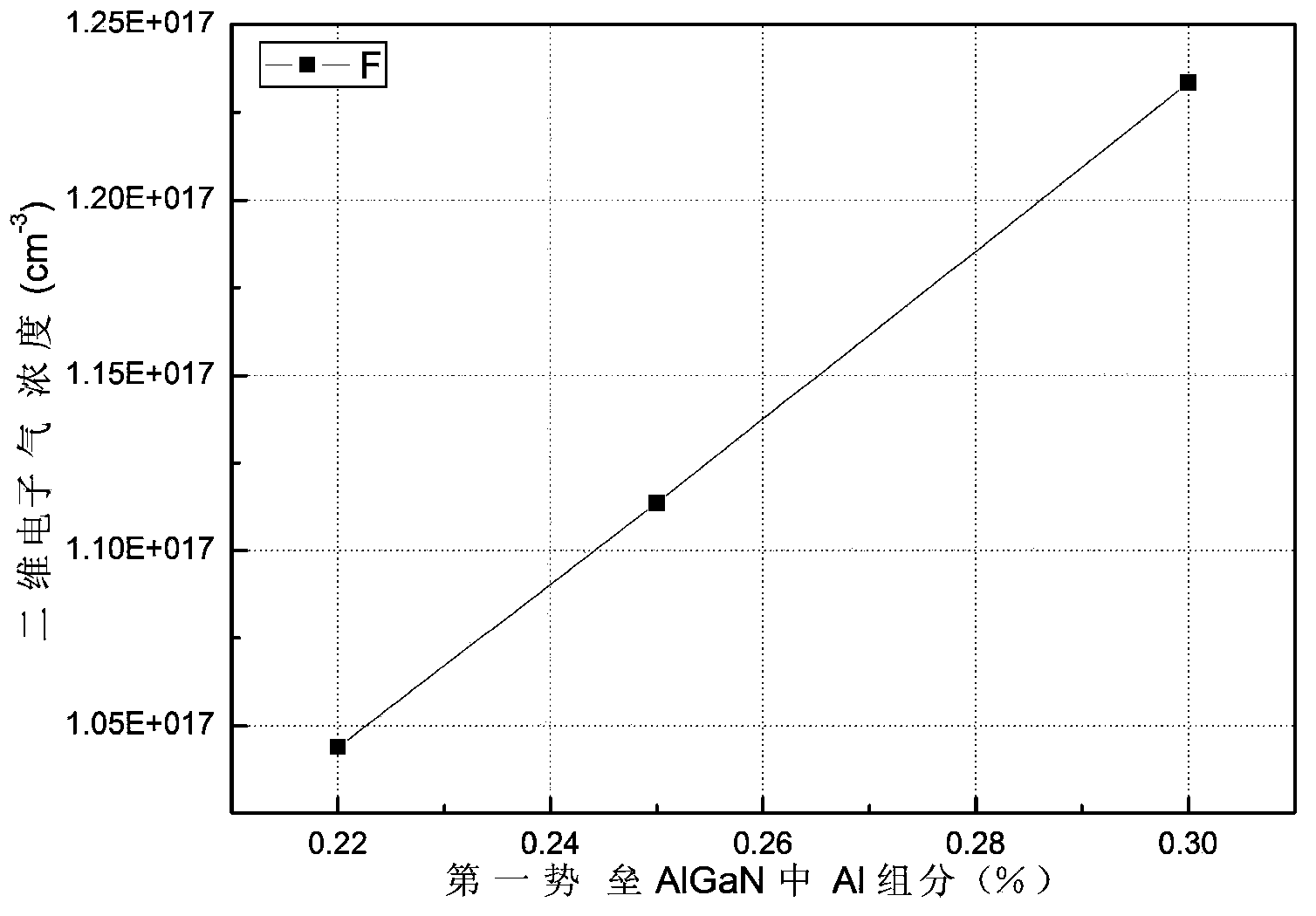
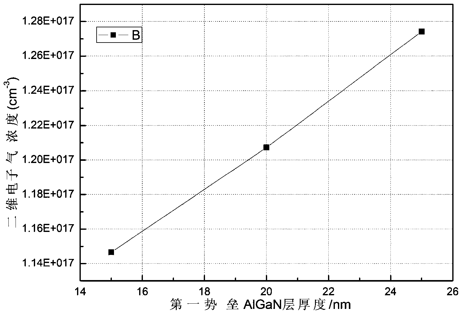
[0043] Double-channel transistor provided by the present invention, see Figure 6 , using GaN as the material, including a double channel, that is, the first channel and the second channel, the first channel is the interface between the barrier layer and the GaN channel layer, and the second channel is the back barrier layer and the GaN channel The materials of the interface of the channel layer, the potential barrier layer and the back barrier layer are all AlGaN; the thickness of the AlGaN back barrier layer is 20nm, and the aluminum composition is 30%. The AlGaN barrier layer has a thickness of 20 nm and an aluminum composition of 30%...


PUM

PropertyMeasurementUnit
Thicknessaaaaaaaaaa
Thicknessaaaaaaaaaa
Thicknessaaaaaaaaaa

Abstract

The invention discloses a double-channel transistor. The double-channel transistor is made of GaN (gallium nitride), and includes two channels, i.e. a first channel and a second channel, wherein the first channel serves as an interface of a barrier layer and a GaN channel layer, the second channel serves as an interface of a back barrier layer and the GaN channel layer, and the barrier layer and the back barrier layer are both made of AlGaN (aluminum gallium nitride); the thickness of the AlGaN back barrier layer is 20 nm, and the aluminum content is 30 percent; the thickness of the AlGaN barrier layer is 20 nm, and the aluminum content is 30 percent; a substrate of the transistor is a silicon carbide substrate. The double-channel transistor and a preparation method for the double-channel transistor have the advantages that AlGaN with a certain aluminum content and a certain thickness serves as the back barrier layer, so as to form an AlGaN/GaN/AlGaN double heterostructure; a two-dimensional electron gas (2DEG) in the channels is confined in two extremely high barriers through a strong polarization electric field to form the two channels, which improves the 2DEG carrier confinement in the channels and the device reliability.

Description

technical field [0001] The invention relates to the technical field of semiconductors, in particular to a high-reliability high-electron-mobility double-channel transistor and a preparation method thereof. Background technique [0002] Aiming at the problem that electrons in the channel of a single heterojunction device tend to overflow under high field and high voltage, thereby reducing the reliability of the device. For single heterojunction devices, the reliability of the device under high field and high voltage is mainly improved through the design of the device structure, such as passivation and increasing the field plate, but the improvement of the device structure and process is inevitable. The introduction of parasitic parameters will lead to the disadvantages of reducing the frequency and efficiency of the device. Therefore, starting from the material structure and fundamentally improving the reliability of the device under high voltage and high field is an effectiv...

Claims


Application Information

Patent Timeline
IPC IPC(8): H01L29/778H01L29/10H01L21/335
CPCH01L29/1029H01L29/66462H01L29/7783
Inventor 赵妙郑英奎刘新宇彭铭曾李艳奎欧阳思华魏珂
Owner INST OF MICROELECTRONICS CHINESE ACAD OF SCI
Why Eureka
Try Eureka