

Epitaxial structure for nitride high electron mobility transistors of composite buffer layers
A high electron mobility, composite buffer layer technology, applied in the direction of circuits, electrical components, semiconductor devices, etc., can solve the problems of lower efficiency, lower device output power, and affect the application potential of GaNHEMT in the direction of high power, and achieve improved thermal conductivity. , crystal quality improvement, and the effect of reducing self-heating effect
- Summary
- Abstract
- Description
- Claims
- Application Information
AI Technical Summary
Problems solved by technology
Method used
Image

Examples
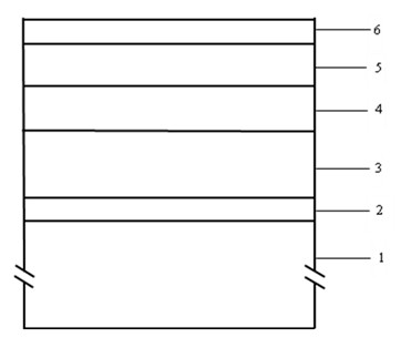
Embodiment 1
[0024] 1) Select a sapphire substrate and grow it using MOCVD technology;
[0025] 2) Baking at 1080°C and 100Torr in a hydrogen atmosphere for 5 minutes;
[0026] 3) Cool down to 550°C, inject ammonia gas and trimethylgallium, and grow a 20nm thick GaN nucleation layer on the substrate surface;
[0027] 4) Raise the temperature to 1080°C, inject ammonia gas and trimethylgallium, and grow 1.0um thick GaN;
[0028] 5) Introduce ammonia, trimethylaluminum and trimethylgallium to grow 1.0um thick composition gradient Al y Ga 1-y N, Al composition y gradually changes from 0 to 0.04 from bottom to top, and 4) GaN constitutes Al y Ga 1-y N / GaN composite buffer layer;
[0029] 6) Turn off trimethylaluminum, grow 200nm thick GaN channel layer at 1080°C;
[0030] 7) Open trimethylaluminum again, and grow a 25nm thick AlGaN barrier layer;
[0031] 8) Cool down to room temperature.
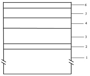
Embodiment 2
[0033] 1) Select a sapphire substrate and grow it using MOCVD technology;
[0034] 2) Baking at 1080°C and 100Torr in a hydrogen atmosphere for 5 minutes;
[0035] 3) Cool down to 550°C, inject ammonia gas and trimethylgallium, and grow a 20nm thick GaN nucleation layer on the substrate surface;
[0036] 4) Raise the temperature to 1080°C, inject ammonia gas and trimethylgallium, and grow 1.0um thick GaN;
[0037] 5) Infuse ammonia, trimethylaluminum and trimethylgallium to grow 1.0um thick Al with constant composition y Ga 1-y N, Al composition y=0.04, and 4) GaN form Al y Ga 1-y N / GaN composite buffer layer;
[0038] 6) Turn off trimethylaluminum, grow 100nm thick GaN channel layer at 1080°C;
[0039] 7) Open trimethylaluminum again, and grow a 25nm thick AlGaN barrier layer;
[0040] 8) Cool down to room temperature.
Embodiment 3
[0042] 1) Select the SiC substrate and grow it using MOCVD technology;
[0043] 2) Baking at 1080°C and 100Torr in a hydrogen atmosphere for 10 minutes;
[0044] 3) At 1150°C, inject ammonia gas and trimethylaluminum, and grow a 50nm thick AlN nucleation layer on the substrate surface;
[0045] 4) Cool down to 1080°C, inject ammonia and trimethylgallium, and grow 1.2um thick GaN;
[0046] 5) Introduce ammonia, trimethylaluminum and trimethylgallium to grow 0.8um thick composition gradient Al y Ga 1-y N, Al composition gradually changes from 0 to 0.05 from bottom to top, and 4) GaN forms an AlGaN / GaN composite buffer layer;
[0047] 6) Turn off trimethylaluminum, grow 100nm thick GaN channel layer at 1080°C;
[0048] 7) Open trimethylaluminum again, grow 20nm thick AlGaN barrier layer at 1080°C;
[0049] 8) Cool down to room temperature.
PUM
| Property | Measurement | Unit |
|---|---|---|
| Thickness | aaaaa | aaaaa |
| Thickness | aaaaa | aaaaa |
| Thickness | aaaaa | aaaaa |
Abstract
Description
Claims
Application Information