
Epitaxial structure for nitride high electron mobility transistors of composite buffer layers

A high electron mobility, composite buffer layer technology, applied in circuits, electrical components, semiconductor devices, etc., can solve the problems affecting the application potential of GaN HEMT in the direction of large power, the output power of the device, and the efficiency. Effects of improved thermal conductivity and improved crystal quality

Active Publication Date: 2015-01-28
NO 55 INST CHINA ELECTRONIC SCI & TECHNOLOGYGROUP CO LTD
View PDF1 Cites 0 Cited by
  • Summary
  • Abstract
  • Description
  • Claims
  • Application Information

AI Technical Summary

Problems solved by technology

Due to the low thermal conductivity of the AlGaN buffer layer, the output current of the device decreases with the increase of the drain bias voltage, resulting in a decrease in the output power of the device and a decrease in efficiency, which affects the application potential of GaN HEMT in the direction of high power

Method used


Image

  • Epitaxial structure for nitride high electron mobility transistors of composite buffer layers

Examples


Embodiment 1

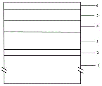
[0024] 1) Select a sapphire substrate and grow it using MOCVD technology;

[0025] 2) Baking at 1080°C and 100Torr in a hydrogen atmosphere for 5 minutes;

[0026] 3) Cool down to 550°C, inject ammonia gas and trimethylgallium, and grow a 20nm thick GaN nucleation layer on the substrate surface;

[0027] 4) Raise the temperature to 1080°C, inject ammonia gas and trimethylgallium, and grow 1.0um thick GaN;

[0028] 5) Introduce ammonia, trimethylaluminum and trimethylgallium to grow 1.0um thick composition gradient Al y Ga 1-y N, Al composition y gradually changes from 0 to 0.04 from bottom to top, and 4) GaN constitutes Al y Ga 1-y N / GaN composite buffer layer;

[0029] 6) Turn off trimethylaluminum, grow 200nm thick GaN channel layer at 1080°C;

[0030] 7) Open trimethylaluminum again, and grow a 25nm thick AlGaN barrier layer;

[0031] 8) Cool down to room temperature.

Embodiment 2

[0033] 1) Select a sapphire substrate and grow it using MOCVD technology;

[0034] 2) Baking at 1080°C and 100Torr in a hydrogen atmosphere for 5 minutes;

[0035] 3) Cool down to 550°C, inject ammonia gas and trimethylgallium, and grow a 20nm thick GaN nucleation layer on the substrate surface;

[0036] 4) Raise the temperature to 1080°C, inject ammonia gas and trimethylgallium, and grow 1.0um thick GaN;

[0037] 5) Infuse ammonia, trimethylaluminum and trimethylgallium to grow 1.0um thick Al with constant composition y Ga 1-y N, Al composition y=0.04, and 4) GaN form Al y Ga 1-y N / GaN composite buffer layer;

[0038] 6) Turn off trimethylaluminum, grow 100nm thick GaN channel layer at 1080°C;

[0039] 7) Open trimethylaluminum again, and grow a 25nm thick AlGaN barrier layer;

[0040] 8) Cool down to room temperature.

Embodiment 3

[0042] 1) Select the SiC substrate and grow it using MOCVD technology;

[0043] 2) Baking at 1080°C and 100Torr in a hydrogen atmosphere for 10 minutes;

[0044] 3) At 1150°C, inject ammonia gas and trimethylaluminum, and grow a 50nm thick AlN nucleation layer on the substrate surface;

[0045] 4) Cool down to 1080°C, inject ammonia and trimethylgallium, and grow 1.2um thick GaN;

[0046] 5) Introduce ammonia, trimethylaluminum and trimethylgallium to grow 0.8um thick composition gradient Al y Ga 1-y N, Al composition gradually changes from 0 to 0.05 from bottom to top, and 4) GaN forms an AlGaN / GaN composite buffer layer;

[0047] 6) Turn off trimethylaluminum, grow 100nm thick GaN channel layer at 1080°C;

[0048] 7) Open trimethylaluminum again, grow 20nm thick AlGaN barrier layer at 1080°C;

[0049] 8) Cool down to room temperature.


PUM


Abstract

The invention relates to an epitaxial structure for nitride high electron mobility transistors of composite buffer layers, which includes that a growth nucleating layer is arranged on a substrate; a first buffer layer is arranged on the growth nucleating layer; a second buffer layer is arranged on the first buffer layer; a growth channel layer is arranged on the second buffer layer; and a growth barrier layer is arranged on the growth channel layer. The growth method includes baking the substrate at a high temperature in a reaction chamber after the substrate is washed and dried; growing the nucleating layer on the substrate, the first buffer layer on the nucleating layer, the second buffer layer on the first buffer layer, the growth channel layer on the second buffer layer, and the growth barrier layer on the channel layer; and reducing the temperature to the room temperature. The epitaxial structure for nitride high electron mobility transistors of composite buffer layers has the advantages of being still capable of forming conduction band discontinuity with a gallium nitride (GaN) channel layer, enhancing 2 dimensional electron gas (DEG) confinement, improving microwave performances and power characteristics of devices, being capable of improving the heat conductivity of the buffer layer, and effectively reducing self-heating effect of high electron mobility transistors (HEMT) of AlGaN buffer layer. Quality of crystals of AlyGal-yN buffer layer can be effectively improved, and the epitaxial structure is helpful for further improving the performance and reliability of devices.

Description

technical field [0001] The invention relates to a nitride high electron mobility transistor epitaxial structure of a composite buffer layer, and belongs to the technical field of epitaxial growth of semiconductor single crystal thin films. Background technique [0002] Gallium Nitride (GaN)-based High Electron Mobility Field Effect Transistor (HEMT) is a new type of electronic device based on a nitride heterostructure. The unique polarization effect of nitride materials makes a high Concentrated two-dimensional electron gas (2DEG) channel, through Schottky gate voltage control channel electrons to achieve work. The device has excellent characteristics of high frequency and high power, and is widely used in wireless communication base stations, power electronic devices and other fields such as information transmission and reception, energy conversion, etc., in line with the current development concept of energy saving, environmental protection, green and low carbon; GaN HEMT ...

Claims


Application Information

Patent Timeline
Patent Type & Authority Patents(China)
IPC IPC(8): H01L29/20H01L29/201H01L29/06H01L29/778
Inventor 彭大青李忠辉董逊李亮倪金玉张东国
Owner NO 55 INST CHINA ELECTRONIC SCI & TECHNOLOGYGROUP CO LTD
Learn More