Semiconductor device
A semiconductor and conduction technology, applied in semiconductor devices, semiconductor/solid-state device manufacturing, semiconductor/solid-state device components, etc., can solve problems such as current collapse and on-resistance rise
- Summary
- Abstract
- Description
- Claims
- Application Information
AI Technical Summary
Problems solved by technology
Method used
Image

Examples
no. 1 approach )
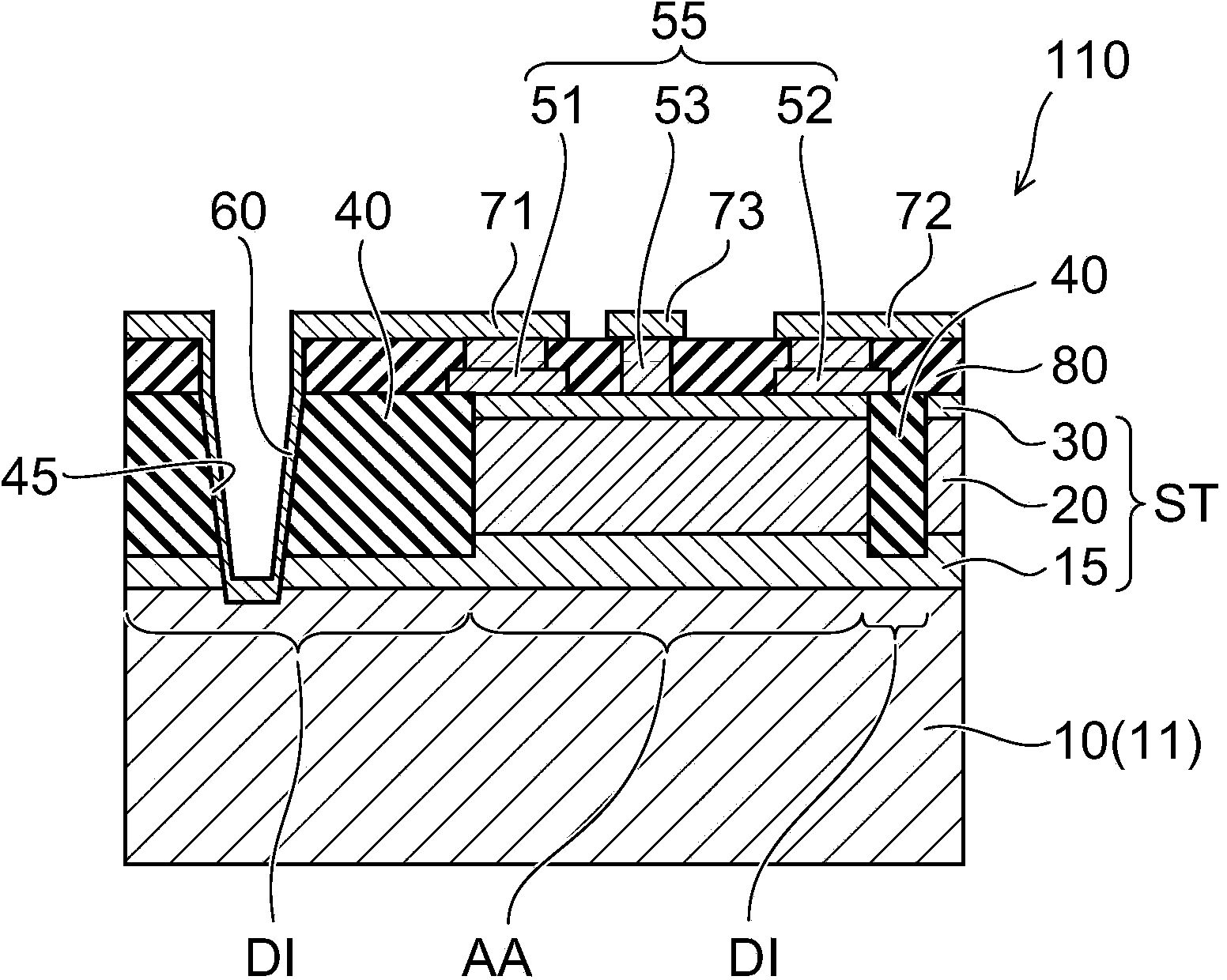
[0029] figure 1 It is a cross-sectional view schematically illustrating the configuration of the semiconductor device according to the first embodiment.
[0030] Such as figure 1 As shown, the semiconductor device 110 according to the first embodiment includes a support substrate 10 , a first semiconductor region 20 , a second semiconductor region 30 , a first electrode 51 , a control electrode 53 , and a conductive portion 60 . The semiconductor device 110 further includes a second electrode 52 . The semiconductor device 110 is, for example, a GaN-based field effect transistor.
[0031] The support substrate 10 includes a conductive region 11 . The conductive region 11 may be provided on a part of the support substrate 10 or may be provided on the entire support substrate 10 . As the supporting substrate 10, for example, a semiconductor substrate (for example, n + type silicon substrate, p + type silicon substrate, n-type silicon carbide substrate) or silicon on insulat...
no. 2 approach )
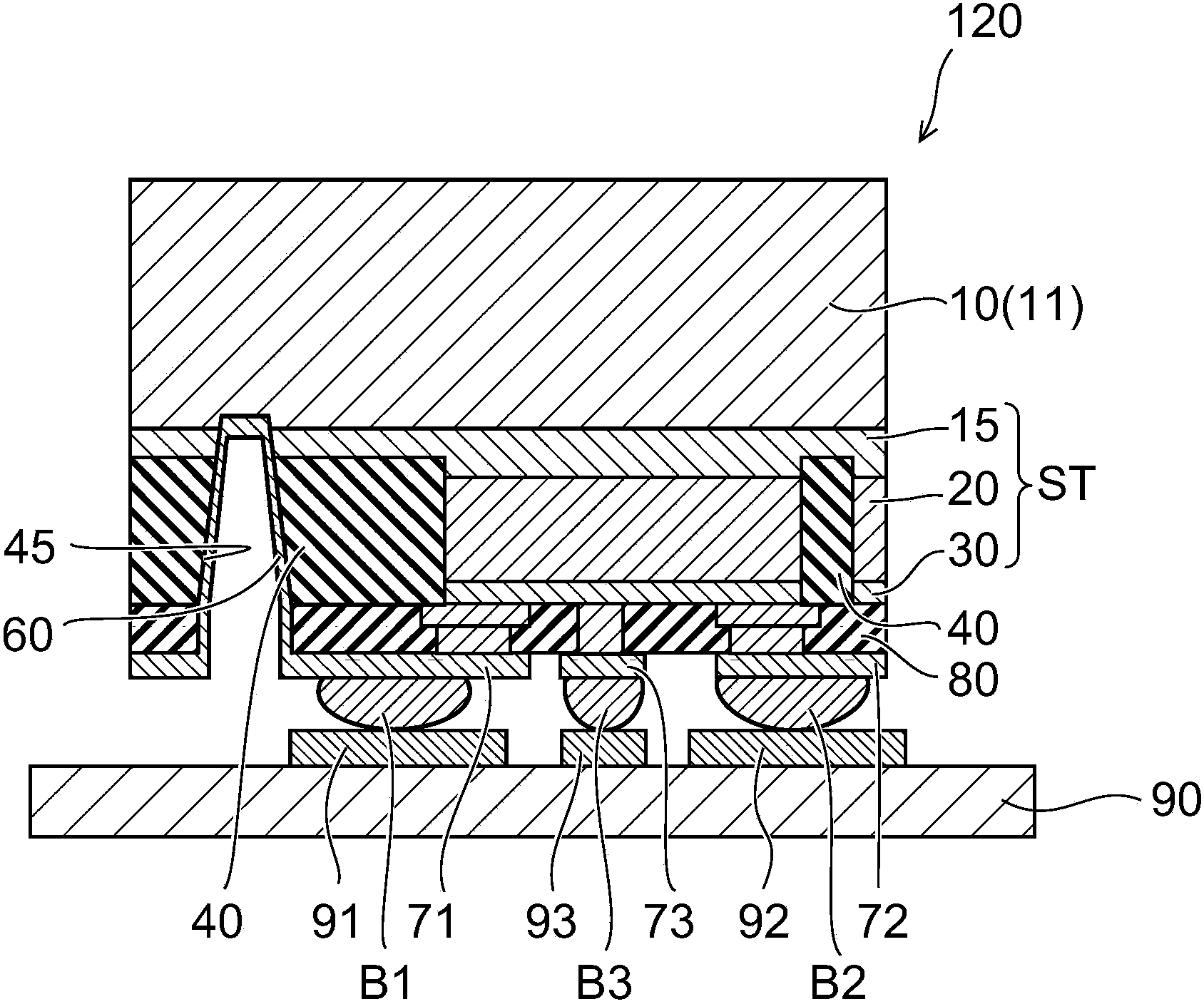
[0047] figure 2 It is a cross-sectional view schematically illustrating the configuration of the semiconductor device according to the second embodiment.
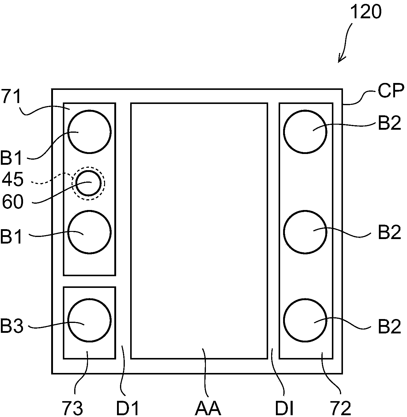
[0048] Such as figure 2 As shown, the semiconductor device 120 according to the second embodiment includes, in addition to the configuration of the semiconductor device 110 according to the first embodiment, bump electrodes (bump electrodes) B1 and B2 respectively provided on the wiring portions 71 , 72 and 73 . and B3. In addition, in figure 2 in, will figure 1 The configuration of the illustrated semiconductor device 110 is shown upside down.
[0049] The bump electrode B1 is provided on the wiring portion 71 conducting to the first electrode 51, the bump electrode B2 is connected to the wiring portion 72 conducting on the second electrode 52, and is connected to the wiring portion 73 conducting on the control electrode 53. There is a bump electrode B3.
[0050] Bump electrodes B1 , B2 , and B3 are connected to w...
no. 3 approach )
[0066] Figure 6A and B are diagrams illustrating the configuration of the semiconductor device according to the third embodiment.
[0067] Figure 6A is a schematic cross-sectional view of a semiconductor device 130 according to the third embodiment, Figure 6B It is an equivalent circuit diagram of the semiconductor device 130 according to the third embodiment.
[0068] Such as Figure 6A As shown, the semiconductor device 130 has a structure in which a plurality of field effect transistors Tr1 and Tr2 are formed on an SOI (Silicon On Insulator) substrate 100 .
[0069] The SOI substrate 100 includes a supporting substrate 10 such as a silicon substrate, silicon oxide (SiO 2 ) and the like, and the conductive region 11 disposed on the insulating layer 12 . The conductive region 11 is, for example, a semiconductor layer with a relatively high impurity concentration (for example, n + shaped silicon layer).
[0070] The semiconductor device 130 is provided with: includin...
PUM
 Abstract
Description
Claims
Application Information
 - R&D
- Intellectual Property
- Life Sciences
- Materials
- Tech Scout
- Unparalleled Data Quality
- Higher Quality Content
- 60% Fewer Hallucinations
Browse by: Latest US Patents, China's latest patents, Technical Efficacy Thesaurus, Application Domain, Technology Topic, Popular Technical Reports.
© 2025 PatSnap. All rights reserved.Legal|Privacy policy|Modern Slavery Act Transparency Statement|Sitemap|About US| Contact US: help@patsnap.com