Supercharge Your Innovation With Domain-Expert AI Agents!

Manufacturing method for forming conductor circuit on non-conductive substrate

A conductor circuit and manufacturing method technology, applied in the direction of removing conductive materials by chemical/electrolytic methods, can solve the problems of high material control and process technology integration capabilities, high technical thresholds, etc., to shorten the manufacturing process and development cycle, The effect of reducing cost and improving bonding strength

Inactive Publication Date: 2014-03-26
KUNSHAN LIANTAO ELECTRONICS CO LTD
View PDF4 Cites 4 Cited by
  • Summary
  • Abstract
  • Description
  • Claims
  • Application Information

AI Technical Summary

Problems solved by technology

However, its material control and process technology integration capabilities are relatively high, which makes the technical threshold for entering the DPC industry and stable production relatively high

Method used


Image

  • Manufacturing method for forming conductor circuit on non-conductive substrate
  • Manufacturing method for forming conductor circuit on non-conductive substrate
  • Manufacturing method for forming conductor circuit on non-conductive substrate

Examples


Embodiment Construction

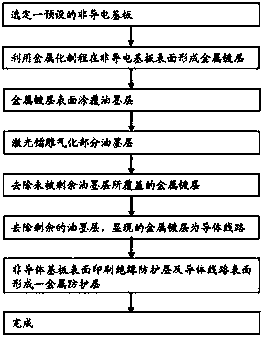
[0025] In order to further have a clearer and more detailed understanding of the purpose, technical solutions and advantages of the present invention, the present invention will be described in detail below in conjunction with the accompanying drawings and specific embodiments.

[0026] Please refer to Figure 1 to Figure 8 As shown, the manufacturing method for forming the conductor line 40 on the non-conductive substrate 10 of the present invention includes the following steps:

[0027] a. A non-conductive substrate 10 is selected, and the non-conductive substrate 10 is made of one of alumina, aluminum nitride and silicon carbide ceramic materials. In other embodiments, the non-conductive substrate 10 is one of thermally conductive plastic, glass or carbon fiber, and the present invention has no special requirements for the material of the non-conductive substrate 10 .

[0028] b. Through the metallization process on the surface of the above-mentioned non-conductive substra...


PUM

PropertyMeasurementUnit
wavelengthaaaaaaaaaa

Abstract

Provided is a manufacturing method for forming a conductor circuit on a non-conductive substrate. The manufacturing method comprises the following steps: a. one non-conductive substrate is selected; b. a metal cladding layer is formed on the surface of the non-conductive substrate; c. an ink layer is coated on the surface of the metal cladding layer; d. partial ink layer is removed after being gasified via a laser technology so that the partial metal cladding layer covered by the partial ink layer before removal appears, and the metal cladding layer under the residual ink layer is still covered by the ink layer; e. the whole system is put in etching liquid so that the appeared metal cladding layer reacts with the etching liquid and is removed, and the metal cladding layer under the ink layer which is not removed is blocked to be contacted with the etching liquid by the residual ink layer so that the metal cladding layer is retained; and f. the whole system is put in acidic or alkaline medicinal liquid so that the residual ink layer is removed, the retained metal cladding layer appears, and the retained metal cladding layer is the finally formed conductor circuit and thus manufacturing of forming the conductor circuit on the non-conductive substrate is completed.

Description

technical field [0001] The invention relates to a manufacturing method for forming conductor lines on a non-conductive substrate. Background technique [0002] Due to the rapid development of the LED (light-emitting diode) electronics industry, the circuit density on the circuit board is getting higher and higher, resulting in more and more heat accumulated on the circuit board during use, and it is becoming more and more difficult to dissipate. , If the heat energy generated by the LED light cannot be exported, the temperature of the LED junction will be too high, which will affect the product life cycle, luminous efficiency, stability, etc. [0003] To improve the luminous efficiency and service life of LEDs, solving the heat dissipation problem of LED products is one of the most important issues at this stage. The development of the LED industry also focuses on high-power, high-brightness, and small-size LED products. Therefore, providing products with High heat dissipat...

Claims


Application Information

Patent Timeline
Patent Type & Authority Applications(China)
IPC IPC(8): H05K3/06
Inventor 李斌汪东平
Owner KUNSHAN LIANTAO ELECTRONICS CO LTD
Features
  • R&D
  • Intellectual Property
  • Life Sciences
  • Materials
  • Tech Scout
  • Unparalleled Data Quality
  • Higher Quality Content
  • 60% Fewer Hallucinations
Learn More